
.jpg?1681996829)
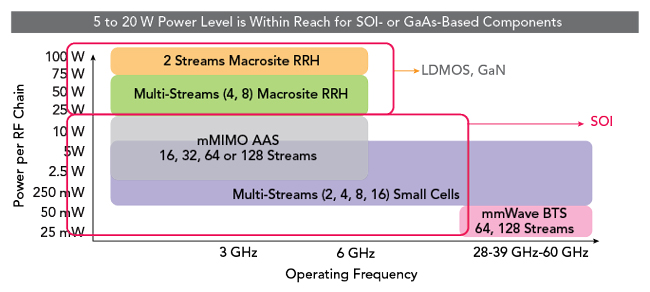
Figure 5 RF power per chain versus operating frequency.
Despite the performance benefits of AAS, there are trade-offs. The mMIMO AAS are much more complex with more internal components and routing considerations, which can make them more expensive. The enhanced performance requires more baseband and antenna processing capabilities, which can make an AAS architecture larger and heavier than traditional PAS architectures that cover the same frequencies.
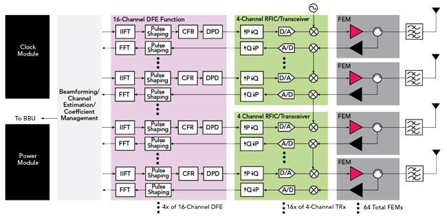
Figure 6 64-channel MIMO RRU architecture.
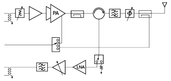
Figure 7 Front-end module architecture.
Historically, wireless base stations have relied on RF transmit chains with output powers typically above 20 W. Power amplifiers (PAs) were fabricated with LDMOS, GaAs and more recently, GaN technologies. As higher-order AAS deploys, RF power levels per signal chain decrease and this opens opportunities for other semiconductor technologies. Figure 5 shows RF power versus operating frequency for several base station configurations. The move toward mMIMO AAS is shifting the RF power market share away from LDMOS and GaN to lower-power technologies like SOI and GaAs. These opportunities arise as the industry appears to be converging on 32T32R and 64T64R as the wireless infrastructure architecture as shown in Figure 6. Figure 7 shows more detail on the front-end module (FEM) and we see the need for switches, amplifiers, attenuators and phase shifters.
AAS HERALD SOI OPPORTUNITIES
As wireless infrastructure architectures move toward mMIMO in AAS, RF designers face challenges designing, developing and fabricating RF components and antenna systems. mMIMO AAS contain more components and they are more complex to meet increasing performance demands, but subscriber revenue growth has been sluggish. Operators are struggling to maximize their return on investment and this places substantial price pressure on system and component OEMs.
There are other ramifications. The RF power per transceiver is lower, but there are many more transceivers, which require more digital baseband processing, and this increases power consumption, footprint and weight. This has direct implications for operating expense and size, pressuring RF component manufacturers to develop more efficient and more highly integrated solutions. These factors are making SOI technology a more compelling solution for wireless infrastructure applications.
RF SOI PRIMER & ADVANTAGES
SOI technology involves fabricating silicon semiconductor devices in a layered silicon insulator-siliconsubstrate. This approach improves performance by reducing parasitic capacitance within the device and to the substrate. SOI technology enjoys higher isolation, linearity, transit frequency and lower loss passive devices compared to silicon. SOI technology uses a process similar to bulk CMOS, benefiting from larger wafer sizes and well-established fabrication verticals. Despite using a silicon process, SOI transistors are not susceptible to latch-up like silicon transistors.
Stacking also increases the power handling capability of SOI technology. Transistor stacking increases the maximum voltage a process can handle by “floating” a series of transistors, each with a limited maximum voltage handling capability. Ideally, the maximum voltage of a stack of transistors would be the maximum voltage of each transistor times the number of stacked transistors, allowing virtually any maximum voltage. However, the parasitic capacitance to the substrate (Csub) with stacked transistors degrades the overall power handling of the stack. The higher the Csub, relative to the gate-drain capacitance (Cgd) and the gate-source capacitance (Cgs), the more the stacking performance degrades. Fortunately, the very low Csub of SOI technology enables very efficient stacking compared to other technologies.
SOI OPPORTUNITIES IN SUB-6 GHZ 5G BASE STATIONS
Figure 8 shows the typical performance requirements of an RRH base station in a sub-6 GHz AAS base station. The lineup highlights the typical semiconductor technology for each function. Assuming a typical receiver IC input and transmitter IC output power of 0 dBm and average radiated output power at the antenna of 320 W, or 55 dBm, limits the range of preferred technologies. LDMOS devices in a Doherty amplifier topology exhibiting a peak-to-average power ratio of 10 dB are the preferred final-stage solution for the amplifier. The peak output power of the PA will be at least 65 dBm and the gain of this stage is likely to be relatively low to support the high power level. Multiple gain stages are used to produce the required output power since each stage will have limited gain. Given the cascade requirements, the transmit (Tx) gain block is the only candidate for SOI technology. In this analysis, GaAs amplifiers support the driver stages to the output PA. A coupler at the PA output provides feedback for the digital predistortion (DPD) circuitry that enhances transmitter linearity and efficiency. This topology has a circulator at the antenna port to route the Tx and receive (Rx) signals and a receiver protection circuit, typically a high-power, non-SOI PIN diode, at the receiver low-noise amplifier (LNA) input. The Rx signal chain uses GaAs LNAs and gain blocks for the noise figure (NF) performance of that technology.
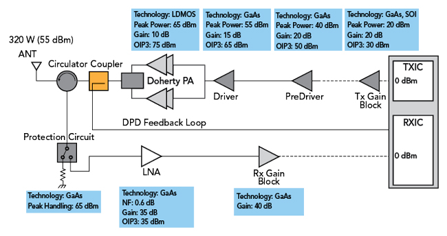
Figure 8 RRH RF lineup.
While the RRH block diagram did not have many opportunities for SOI technology, the mMIMO AAS lineup shown in Figure 9 does. The radiated power from each antenna in this example is 10 W, but the total radiated power remains the same as in the earlier example. With peak PA output power at 50 dBm, the output stage can be GaN or GaAs technology with higher gain. An SOI digital step attenuator (DSA) may be used after an SOI Tx gain block for beam adjustment. Multiple transceivers means multiple PA output couplers for DPD feedback and these couplers can feed an array of SOI SP4T switches. With lower power in each transceiver, the Rx signal chain protection circuit can be realized with SOI. A GaAs LNA is still desirable for low NF performance, but SOI can be used for the level-controlling Rx gain block and DSA at the receiver input. SOI switched-filter banks may be used at the transceiver input to enhance selectivity and output performance. SOI exhibits high power handling, high isolation and excellent linearity performance, making it particularly well-suited for switching applications. Unlike the RRH example, mMIMO AAS base station configurations will present many RFFE SOI opportunities and these are shown in green in Figure 9.
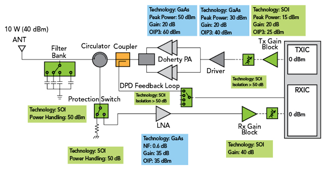
Figure 9 32T32R AAS base station RF lineup. Source: “Massive MIMO, mmWave and mmWave-Massive MIMO Communications: Performance Assessment with Beamforming Techniques” Tewelgn Kebede Engda, et al.
SOI OPPORTUNITIES FOR 5G BEAMFORMERS
Beamforming is essential for high gain and directivity in mMIMO antenna arrays. The three primary beamforming techniques are analog, digital and hybrid. A digital beamformer processes each RF stream in digital blocks, with a dedicated conversion block per line. An analog beamformer processes a single stream in the baseband, with beamforming accomplished with attenuators and phase shifters at the antenna elements. A hybrid beamformer groups antenna elements into blocks and assigns a digital stream to each block. In this scheme, each element has an analog phase shifter and attenuator. Each beamforming topology has advantages and trade-offs as shown in Table 1.
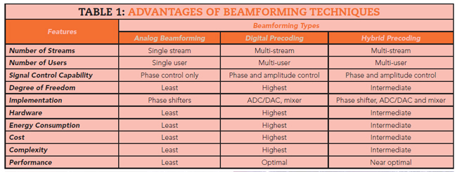
A digital beamformer offers the highest degree of flexibility, data throughput and coverage since each RF transceiver has a dedicated stream that is processed simultaneously. This requires an enormous amount of processing and a dedicated RF connection to each antenna element. An analog beamformer has the least complexity and power consumption, but it sacrifices flexibility and capability. A hybrid beamformer represents a compromise between the flexibility and performance of a digital beamformer and the simplicity and lower power consumption of an analog beamformer. Figure 10 compares a digital beamformer with a hybrid beamformer, with both having four RF lines. The hybrid beamformer in this example has one digital data stream that is distributed to the antenna elements through four phase shifters and eight switches. This architecture consumes roughly one-quarter the power of an equivalent digital beamformer. The hybrid solution is likely to be smaller, weigh less and have a lower cost than a digital beamforming solution. The disadvantage of this approach is only one independent data stream versus four streams in the digital beamformer.
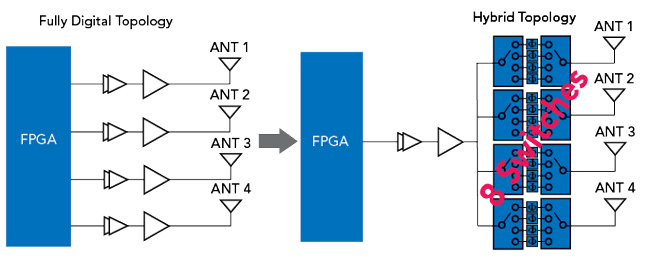
Figure 10 Comparison of digital and hybrid beamformer topologies.
CONCLUSION
5G mMIMO base station deployment is ramping up and operators and equipment manufacturers are moving away from the legacy components and designs of earlier cellular telecommunication generations. New mMIMO architectures require dramatically different components than legacy base stations and this necessitates an evolution of the wireless technology. The new base stations have many more RF lines, with each line requiring lower RF transmit power. As 5G mMIMO system requirements evolve, OEMs and RF component vendors will collaborate to develop and optimize performance to achieve better power efficiency, size, weight and cost. These efforts will likely require greater levels of integration and fit nicely with the advantages of SOI technologies, setting the stage for an increase in the market share for SOI-based components in wireless base station applications.