
The industry has been talking about the small cell market for many years as being on the verge of huge growth, but while it is a sizable market and there has been some growth, it has not taken off as quickly as many expected. Though with the emergence of 5G, it is poised to do so; meeting the goals of increased capacity in dense areas and the large number of connections needed for IoT applications. In 2020, the 5G small cell market was $741 million and is expected to grow to about $18 billion by 2028, according to Forbes Business Insights, exhibiting a compound average growth rate of 54 percent.
The Small Cell Forum recently published “5G NR FR1 Reference Design, the case for a common, modular architecture” that outlines the design of small cells in detail (Document 251.10.01). This article is based on sections 3.2-3.4, outlining the architectures for the RF section of small cells. Hear from some of the authors of the Small Cell Forum report in this podcast:
The market for small cells is diversifying for use in many cases, deployment models and form factors. According to the report, with each scenario having its own connectivity requirements, there is a significant risk of fragmentation, which would make many networks uneconomic. This risk can be eliminated by creating common platforms based on standard interfaces, which enable a wide range of components to interoperate to support diverse small cell designs while retaining economies of scale. This approach is like the Open RAN effort that is being developed at the network level and the Open RF effort to standardize the RF front-end (RFFE).
The interfaces between different vendors’ small cells, or between different functional splits, are not uniform. This can increase cost, complexity, integration time and reduce scale. Common interfaces address the challenge that not every component can be uniform. The biggest issue addressed in the report is that the RFFE will be different, depending on spectrum frequency, output power and other factors. Neutral host and enterprise deployments need to support as many frequencies as possible to accommodate many users, which increases the bandwidth requirement.
According to the Small Cell Forum, the solution to the RFFE issue is a modular approach to small cell network design, in which a variety of RFFE designs can be interfaced in a standardized way, like the baseband and transceiver units. The RFFE can be swapped in and out to support different markets without changing the rest of the platform.
While the report provides the framework for the components and interfaces that make up a 5G NR FR1 small cell distributed radio unit, this article will concentrate on the RFFE FR1 architectures outlined by the Small Cell Forum, since those are the ones of interest to RF designers.
RF TRANSCEIVERS
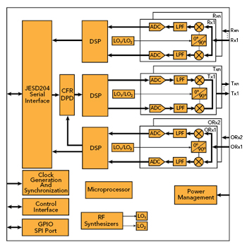
Figure 1 Example of an RF transceiver architecture.
The RF transceivers contain independently controlled transmitters, dedicated observation receiver inputs—for monitoring transmitter channel outputs—independently controlled receivers, integrated synthesizers and digital signal processing to provide a complete transceiver solution as shown in Figure 1. The transceivers support both time-division duplexing (TDD) and frequency-division duplexing (FDD) applications.
To meet the 5G FR1 specifications, the transceiver can operate in a wide frequency band covering a range from 650 MHz to 6 GHz (or higher). Depending on the number of controlled transmitters and receivers in the single-chip transceiver device (2T2R, 4T4R, etc.), the transceiver bandwidth performance can be specified. One or two observation receiver channels can monitor feedback from the transmitter outputs. The feedback loop can be used to implement error correction, calibration and signal enhancing algorithms, such as crest factor reduction and digital predistortion (DPD). The observation receivers operate in the same frequency range as the transmitter channels and can support a channel bandwidth up to more than 2x the transmitter bandwidth.
To improve transmitter dynamic range, the transceiver can provide a power control range using variable attenuator(s). To achieve a high level of RF performance, the transceiver includes integrated phase-locked loops (PLLs). The PLLs provide low noise RF synthesis for the transmitter and receiver signal paths, support an independent frequency for the observation receiver and generate clocks for the converter and the digital circuits for signal processing and communication interfaces.
RFFE
The RFFE in a small cell radio provides the following functionality:
- It sequentially or simultaneously boosts up the power of the transceiver output signal and amplifies the received signal from the user equipment (UE) based on the control from the baseband or the RF transceiver.
- It provides the transmitter observation path to the RF transceiver to further improve the linearity of the entire transmitting path, based on the digital algorithm/calibration, i.e., DPD.
- It filters out the harmonic or intermodulation signals on the transmit path and the jamming or interfering signals on the receive path.
To accomplish this functionality and to optimally balance cost and performance, current RFFE implementations typically fall into heterogeneous integration, which involves multiple discrete active and passive components fabricated by different technologies. For example, the power amplifier (PA) is usually implemented in GaAs, GaN or LDMOS processes because the transistor breakdown voltage is multiple times higher than the CMOS process for generating the desired output power efficiently.
The low noise amplifier (LNA), the first amplifier on the receive path, should ideally have a noise figure (NF) lower than 1 dB and an input third-order intercept point to meet the sensitivity and blocking requirements in the small cell. The PHEMT-based LNA is a common choice due to its low NF and sufficiently high operating voltage.
In the filters, the passband loss, the rejection outside the passband and power handling are the three key parameters in the component selection. The acoustic wave filters, including surface acoustic wave and bulk acoustic wave, are currently the popular choice for the receive path due to their high rejection with a small footprint. The ceramic-type filter is typically chosen to connect the RFFE to the antenna, as its power handling is greater than that of acoustic filters.
Based on the current 3GPP definition, there are more than 20 frequency bands for sub-6 GHz 5G. This implies that RFFE hardware will be band selective. The component suppliers will typically try to develop multiple products in a pin-to-pin-compatible family to cover the entire sub-6 GHz bands to minimize RFFE hardware changes when changing frequency bands. In addition, the number of transmitting and receiving paths in the RFFE needs to be scalable by two to meet the desired MIMO configuration, i.e., 2T2R, 4T4R and 8T8R.
The RF transceiver is responsible for converting the digital baseband signals to analog signals at the desired frequency. Most available 5G NR FR1 transceiver ICs are based on a CMOS process, can operate up to 6 GHz to cover the entire FR1 spectrum and support at least 4T4R in a signal IC. (FR1 was changed to 7 GHz but most still refer to it as up to 6 GHz). Some transceivers further integrate digital functions to implement algorithms to calibrate or improve the entire signal chain, e.g., linearity, image rejection, leakage reduction and spurious filtering.
The baseband function is almost entirely digital, configured by software and independent of RF frequency. Baseband components include digital processors, memory and interface components. Small cell radio units designed for high volume markets may integrate all functions onto a single printed circuit board (PCB) for lowest cost. Alternatively, some lower volume markets may be addressed more economically using a modular solution; for example, integrating the interfaces, power, baseband and RF transceiver functions onto one PCB serving multiple markets; while band-specific components are grouped into a separate market-specific RFFE module (FEM).
FUNCTIONAL BLOCK TDD
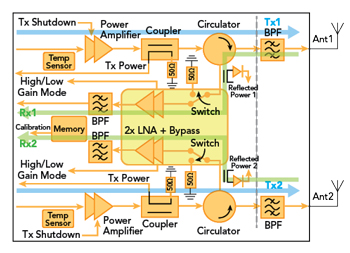
Figure 2 Small cell RFFE components in TDD mode.
Figure 2 shows a transmitter/receiver with two observation path RFFEs in TDD for sub-6 GHz 5G. TDD means both transmitter and receiver operate alternately in the same frequency band. Ideally, in a 2T2R configuration, the two transmitting paths are identical; the same holds for the receiving and observing paths. All the RF components in the RFFE interface to each other in a 50 Ω system. The observing path, implemented by the directional coupler, couples a small amount of output power from the PA and feeds it into the transceiver for signal analysis and processing. This enables the transceiver to accurately monitor and control the output power, as well as applying DPD to improve the linearity of the transmit signal. The operating frequency of the observing path is typically identical to that of the transmit path.