
The PA is typically a GaAs-based, high efficiency amplifier that uses the DPD algorithm from the transceiver or baseband to deliver adequate output power with high efficiency and linearity, while reducing the power consumption and heat generation compared to a linear amplifier. The receiver FEM integrates an LNA and a single pole double throw (SPDT) switch into a single component. A single component is favored over a discreet solution, because of improved performance, lower cost and smaller PCB footprint.
The bandpass filter (BPF) between the circulator and antenna port (i.e., the antenna filter) typically helps eliminate harmonic signals generated by the PA and protect the receiving path from interference and jamming. The filter after the LNA, the second filter in the receive path, further suppresses interfering signals from the antenna (ANT) port. The circulator, which is a non-reciprocal component, transmits the PA signal to the antenna while shielding the PA and switch from the reflecting signal from the antenna port, caused by impedance mismatches.
Some systems insert a power sensor between the switch and circulator to monitor the input power coming from the ANT port. When the sensor indicates the input power is higher than the expected value, the receiver components can be shut down or bypassed to avoid damage. Both the antenna filter and circulator must handle the output power of the PA without damage.
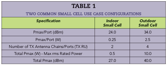
Table 1 shows two of the most typical small cell configurations: one for indoor and one for outdoor. 24 dBm is the required conducted power for the indoor small cell, and the table shows typical line up calculations to illustrate how the RFFE achieves the targeted output power. The analysis is based on typical performance specifications of products generally available in the market, with a few choices made to ensure signal integrity, cost competitiveness and multiple vendors.
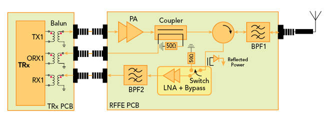
Figure 3 Simplified small cell RF line-up in TDD mode.
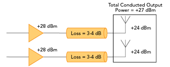
Figure 4 2T2R Indoor Small Cell TX power budget.
For simplicity, the block diagram in Figure 3 only shows a single transceiver RFFE and its interfaces to the transceiver board and external antenna. The passive components and interconnections contribute to loss in the system, as well as path losses. The RF ports of the transceiver are all differential and require passive baluns to connect to the RFFE board. The passive components on the RFFE board include the coupler, circulator and BPFs.
Figure 4 shows the PA output power must be +28 dBm to compensate for filter and antenna losses, ensuring +24 dBm is delivered to the antenna port. Typically, the transceiver can deliver around 4 to 6 dBm power CW. With the peak to average power ratio of the NR signal, targeted DPD expansion and the balun’s loss, the average output power from the transceiver board is about -7 dBm. To deliver 24 dBm to the antenna, the power gain of the PA needs to be at least 35 dB to compensate for the loss of the transmitting path. With DPD, the PA’s saturated output power should be at least 36.25 dBm, with its 1 dB compression point at least 32.25 dBm. More detail about the RFFE transmit and receive line ups are in Table 2.
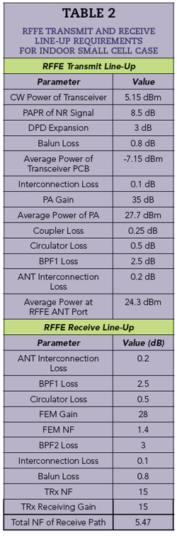
In the receive path, the FEM, which integrates an LNA and SPDT switch into a single component, is the only active component. The typical gain and loss of the extra components, including BPF2, with the FEM and transceiver gain and NFs, are summarized in the table.
Using the equation for NF in a cascaded system, the NF of the entire receive path is about 5.47 dB. The effective receive gain, which is the sum of all gains and losses on the receive path, is 35.9 dB. The total NF can be improved by either using passive components with less loss or increasing the LNA gain.
The temperature sensors in the RFFE help the system monitor the operating temperature of the RFFE in operation. Multiple temperature sensors individually measure the temperatures in different locations, outline the temperature profile of the RFFE and assist with making electrical adjustments to minimize RFFE temperature variants, or shutting down the hardware if the RFFE is overheating.
The memory inside the RFFE stores the following information to help the small cell in system initialization, online or offline calibrations.
- Hardware manufacturing information
- RFFE electrical characteristics, including linear and non-linear types
- Performance variants due to frequency, temperature and bias dependence.
FUNCTIONAL BLOCK FDD
Figure 5 shows the FDD RFFE block diagram. The dashed line in the figure indicates the boundary between the RFFE and two duplexers in a 2T2R configuration. The diagram on the left side of the line is identical to the same portion of the TDD RFFE, except for the connections of the circulators and switch. This design approach consequently unifies the RFFE interface with antennas in the two systems. This methodology can reduce the extra effort when changing the design or implementing a multi-mode small cell to provide TDD and FDD operation in the same hardware.
The operating frequencies of the transmitting and receiving paths in the FDD small cell are different. The observation path needs to be designed at the same frequency as the transmitter, and the frequency of the filter after the LNA needs to match the receive frequency. The data formats for the content inside the memory of the FDD block diagram, compared with the TDD diagram, use different frequency points to record the transmitter’s and receiver’s electrical performances.
Antennas
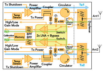
Figure 5 Small cell RFFE components in FDD mode.
The antenna radiates the RF power and receives the signal from the UE. In both TDD and FDD small cells, the transmitting and receiving paths from the same RF transceiver share the same antenna. The number of RF transceiver ports and the polarization diversity of the small cell define the total number of antenna elements connecting to the cell. Based on the system requirements, the antenna can be either omnidirectional, for full 360-degree coverage, or directive, to focus the radiation on narrower angles. The antenna can be planar, realized by a multilayer PCB, and integrated into the RFFE board.
A planar antenna (like a patch, slot and planar inverted-F) typically has a gain of 3 to 7 dBi. 3D antennas are also popular in small cells such as dipole, monopole and helical. These typically use cables or connectors to interface to the RFFE and may be integrated within the small cell radio. If integrated, they may be incorporated onto the PCB without connectors or mounted off-board, in which case flying leads may be soldered or connected using, for example, UFL-style connectors. When the antennas are not integrated, as with higher power outdoor small cells, waterproof RF connectors such as N-type or 4.3-10 may be employed.
CONCLUSION
While the small cell architecture is a little different for FDD versus TDD, many common signal chains can be shared. Standardization of architectures can reduce cost, speed time to market and minimize complexity while diversifying the supply chain. It remains to be seen if standard architectures will be widely adopted, but they are gathering momentum; in either case, the architectures covered here will closely represent the design of small cells for the 5G market.