
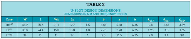
The UMSA is designed using TRF and DI techniques and compared with TCM. Table 2 summarizes the respective design variables with the achieved frequency band of operation. The three respective designs are simulated assuming the infinite substrate boundary conditions in MoM. Table 2 shows good agreement in terms of fres; however, the TCM agrees more closely with DI and yields a much more compact geometry compared to the one achieved using the TRF technique. This is because the DI technique also derives its respective ratios from MoM simulations41; therefore, both DI and TCM consider the fringe fields and finite edge effects. Thus, the design procedure using TCM is validated.
MC Analysis
MC behavior is described in 2 × 1 and 2 × 2 arrays. Figure 7 shows a 2 x 1 array as an inset and plots the self and mutual scattering parameters (SP) versus frequency. Over the 3 to 3.5 GHz band, the coupling |S21| is less than ‐18 dB and |Γ| = |S11| is less than ‐10 dB. Figure 8a shows a 2 × 2 array model and its respective SPs. |Γ| for all ports is less than ‐10 dB and MC is less than ‐18 dB over the 3 to 3.5 GHz band. A little variation in the resonance peaks of the four elements is observed due to the MC effect.17 Figure 8b shows the uniformly fed array radiation pattern. The HPBW is ∼54 degrees, Ge is ∼ 6.9 dBi and the peak sidelobe level is less than ‐13 dB.
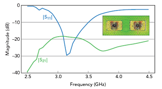
Figure 7 UMSA self and mutual SPs.
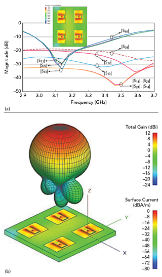
Figure 8 UMSA 2 × 2 array self and mutual SPs (a) and radiation pattern (b).
Annular Ring Design
An annular ring (see Figure 9) is designed with dimensions based on the center frequency36 using (22):

In (22), υ = 3×10⁸ m/s, Lα=LSIW‐(L+2c) = 42.21 mm and Wα = WSIW‐(W+2 d) = 39.21 mm. TCM identifies two resonances, 2.2 and 3.4 GHz for modes J1 and J4 (see Figures 9a and b), respectively. The dominant mode is the TM11 mode (J1) in this structure.
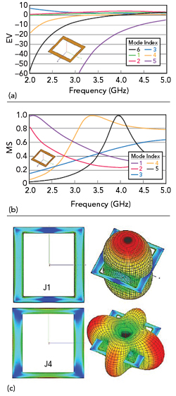
Figure 9 Annular ring EV (a) and MS (b) vs. frequency; surface current distribution and radiation pattern for modes J1 and J4 (c).
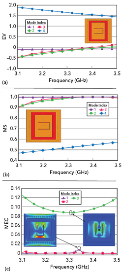
Figure 10 SIW CBMSA TCM EV (a), MS (b) and MEC (c) vs. frequency.
SIW Cavity-Backed UMSA (SIW CBMSA)
The annular ring with a PTH array adjoined to the UMSA (see Figure 1 and Figure 10) forms the SIW CBMSA structure. The dimensions are LSIW = 50.21, WSIW = 50.21, c = 4 and d = 5.5 mm. The PTH diameter is 1 mm, with a spacing of 2.875 mm, optimized to minimize leakage loss based on MC estimation between two adjacent antenna elements.
Figures 10a and b show EV and MS versus frequency considering four CMs, from Equation 12. An enhanced bandwidth is observed, contributed by modes J1, J2 and J3. Figure 10c plots MECs considering probe excitation and shows that J3 is the dominant mode while J1 contributes to a lesser degree.
Figure 11 shows the combined surface current distribution, J1+J3, and associated 3D radiation pattern at 3.3 GHz; normalized phi-cut distributions are also shown. An in-phase coupling between U-slot and patch edges is observed with minimal leakage to the annular ring, thus ensuring isolation from nearby structures. Ge is ∼6.9 dBi and HPBW is greater than 89 and 82 degrees in the respective planes.
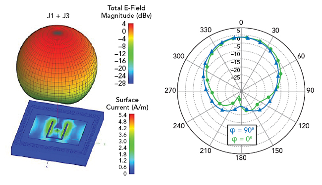
Figure 11 SIW CBMPA radiation pattern and surface current distribution.
A bandwidth of 670 MHz (FBW = ∼20 percent) is shown by the dotted red curve in Figure 12. Figure 12 compares the simulated |Γ| obtained in an isolated environment with an infinite array environment generated using periodic boundary conditions (PBC).17,18 It also compares these with the measured |Γ| in an array environment. Generally good agreement is observed, with a slight difference between the PBC and measured results, due to neglecting the finite edges in the PBC environment.
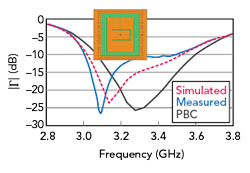
Figure 12 Reflection coefficient magnitude vs. frequency.
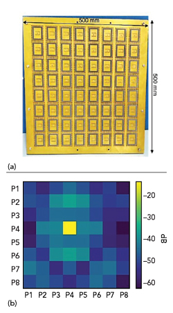
Figure 13 SIW CBMA array (a) and mutual MC variation (b).
MEASURED RESULTS AND DISCUSSION
A 64 (8 × 8) SIW CBMSA array 500 × 500 mm2 in size is fabricated using standard photo-etching techniques. The inter-element spacing is 0.552λo along the x- and y-directions. It has a 5 mm-thick aluminum ground plane while ensuring that no air bubbles are formed in the structure (see Figure 13a).
The central element performance and the MC variation is measured (see Figure 13b). Coupling is measured between the central element and all other array elements. It is observed that the worst coupling is less than ‐20 dB, i.e., minimal leakage occurs from the SIW structure to its neighbors. Figure 12 shows the measured FBW is ∼22.5 percent (∼740 MHz), from 2.96 to 3.7 GHz for a VSWR less than 3:1, and 18 percent (∼600 MHz), from 3 to 3.6 GHz for a VSWR less than 2:1.
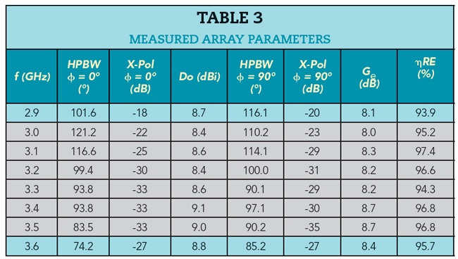
Table 3 summarizes the radiation parameters in the array environment measured in a planar near-field test measurement facility. The variation observed between the measured and the simulated parameters are attributed to the variation in h, due to the bonding of two layers of the substrate using a Rogers 3001 bonding film to achieve the desired thickness. The set targets are met from 3.1 to 3.5 GHz, showing Ge is greater than 8.4 dBi, the efficiency ηRE is greater than 95.2 percent (see Equation 23), cross-polarization is less than ‐22 dB and the HPBW is greater than 90 degrees in both principal planes except near the upper edge of the frequency band.