
The 0.5 mm wide differential audio lines were evaluated to assess the paired lines separation and coupling rate, because positive and negative lines must be tightly coupled within a specific distance. In Table 1, the separation criterion (center-to-center distance of 0.75 mm) was determined by adding the line width (0.5 mm) and the spacing between the lines (0.25 mm). The coupling rate criterion of better than 80 percent was determined by considering the structures of the USB IC and connector. From the verification solver, the maximum separation was 0.893 mm between the two lines, with a coupling rate of 76.6 percent. Referring to Table 1, the criteria were not satisfied. However, the ground shield ratio, which shows the extent the audio lines are shielded by a ground plane, does meet the specification of greater than 80 percent. These results are useful for verifying the layout of the audio lines.
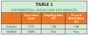
Figure 4 shows the characteristics of the USB data lines (D+/D-) and memory bus lines, studied using the SI solver in PollEx. For the USB study, the ideal digital signal transmitted from the USB IC and received at the USB connector has a pulse width of 2.08 nS, corresponding to a data rate of 480 Mbps, with a peak voltage of 0.4 V. In Figure 4a, the received signals show enough voltage margin for normal USB operation because both the high threshold (0.3 V) and low threshold (0.1 V) USB 2.0 specifications are satisfied.6 Similarly, the memory interface lines between the controller and the pseudo-static random access memory were analyzed (see Figure 4b). For this analysis, one differential clock line and a group of address lines were selected from the PCB design. The controller was assumed to send the clock signal with a frequency of 133 MHz and the address signals at a data rate of 256 Mbps. The eye diagram was simulated at the memory ports. The clock signal is used as a criterion to estimate the interface with the eye mask, whose high and low thresholds are 1.3 and 0.4 V, respectively. Additionally, it is assumed that the required setup and hold times for the interface are 2 and 1.5 nS, respectively. As the eye diagram shows sufficient voltage margin, the interface lines are well routed for reliable 256 Mbps data exchange between the controller and memory.
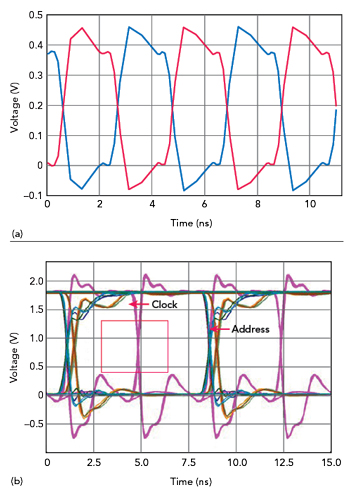
Figure 4 SI results: received signals at USB lines (a) and eye diagram for the clock and address lines of the memory bus (b).
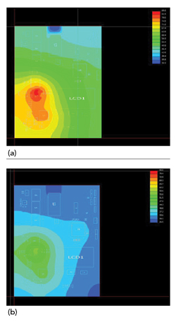
Figure 5 PCB surface thermal contours with natural convection (a) and forced air (b).
A board thermal analysis was performed to check the main audio amplifier’s operating temperature, using the amplifier’s quad flat package and 5 W power rating at room temperature. Figure 5 shows the temperature contours for two conditions: 1) natural convection (see Figure 5a) and 2) forced air convection with an air flow of 5 m/s (see Figure 5b). With natural convection, the highest temperature of 85°C is the maximum allowed for normal amplifier operation. Forced convection decreased the temperature from 85°C to 59°C, which improves reliability.
ANTENNA DESIGN AND INTEGRATION
The antenna design was inspired from the meander line antenna (MLA) concept proposed by Rashed and Tai.7 The antenna was integrated on the PCB and placed in its working environment within the speaker assembly to identify the optimal location. Antenna electromagnetic (EM) characteristics in different configurations changing the location and orientation of the PCB inside the speaker cabinet were simulated using the 3D high frequency EM simulation tool, Altair Feko.8
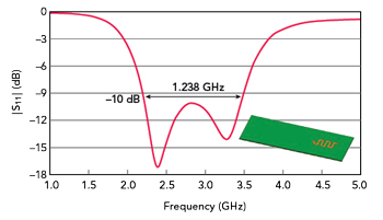
Figure 6 |S11| of the MLA designed for BT.
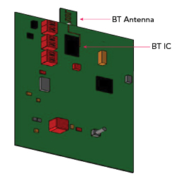
Figure 7 MLA integrated with the BT PCB.
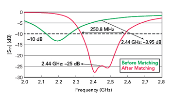
Figure 8 |S11| of the MLA integrated with the PCB.
Meandering the antenna increases the surface current path and enables reducing the antenna size. The resonant frequency of an MLA is a function of the meander separation and meander spacing; the resonant frequency can be reduced by increasing the meander separation, and vice versa.9 As shown in Figure 6, the simulation showed the magnitude of the reflection coefficient of the MLA design on an FR4 substrate was approximately -17 dB at 2.4 GHz. The MLA integrated on the BT PCB is shown in Figure 7. The components on the PCB surrounding the antenna alter its resonance characteristics significantly (see Figure 8), requiring a matching circuit to restore the performance. The matching circuit comprises a simple LC network with a 0.778 pF series capacitor and a 53 nH shunt inductor, which shifts the resonance back into the BT frequency range.
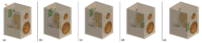
Figure 9 Antenna locations within the speaker cabinet: 1 (a), 2 (b), 3 (c), 4 (d) and 5 (e).
The speaker cabinet is made of balsa wood with a dielectric constant of 1.3 and dimensions of 355 × 305 × 450 mm. In addition to the PCB, the components inside the speaker include a cooling fan, metallic heat exchanger, acoustic port and the speaker module. The location and orientation of the PCB are influenced by the spacing inside the cabinet, mounting support options and thermal efficiency. Taking these into account with the physical constraints, a complete in-situ analysis of the speaker assembly was performed considering several locations and orientations (see Figure 9). Location 1 places the antenna near the back wall of the speaker facing outward, i.e., toward the back side. Locations 2 and 3 mount the PCB on the same back wall facing inward, with the antenna pointed up and down, respectively. Locations 4 and 5 mount the PCB in free space between the components, facing inward and close to the back and front walls, respectively. Comparing the five positions, the magnitude of the reflection coefficient is less than -10 dB for all the locations except 1 (see Figure 10). The 3D radiation patterns (see Figure 11) show that locations 2 and 3 have nearly omnidirectional coverage along the horizon, which is required for good BT performance. Location 2 was chosen for the next step of the analysis, evaluating BT wireless coverage and the speaker’s coexistence with Wi-Fi.
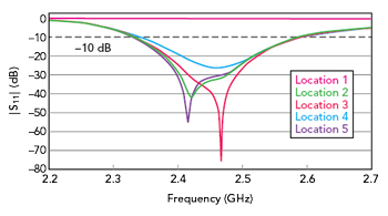
Figure 10 MLA |S11| for locations 1 to 5.
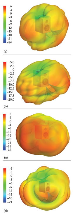
Figure 11 3D radiation patterns showing the total realized gain (dBi) for locations 2 (a), 3 (b), 4 (c) and 5 (d).
WIRELESS COVERAGE AND INTERFERENCE
With the advent of 5G and IoT, the trend is toward smart household electronics, including speakers. These smart devices use standards such as Wi-Fi, BT, LTE and ZigBee for connectivity, and some of these technologies operate in closely separated frequency bands, which can cause interference.10 BT and Wi-Fi, for example, operate around 2.4 GHz and coexist, although interference from BT can reduce Wi-Fi throughput and vice versa. Analyzing interference through virtual prototyping early in the design stage can avoid costly rework later.