
Widespread deployment of 5G networks will enable tremendous advancements in connectivity and communications, by increasing bandwidth 10x and reducing latency 50x. Hyperscale datacenters are major beneficiaries of this improved performance, from the cloud computing and storage of massive amounts of data generated by 5G applications. Such improvements in speed and latency require significant improvements in the equipment and components used in datacenters; however, because datacenters have limited space and are expensive to expand, newer generation equipment and components must increase data rates while minimizing any increase in size. Another requirement is minimizing power consumption, as the power needed to operate datacenters is extraordinary—projected to consume as much as eight percent of global electricity usage by 2030, according to the sustainable information and communications technology expert Anders Andrae.
Optical transceivers, which connect and translate data carried over optical fibers into electrical signals within the datacenters, are one of the most important devices in the network connecting users to datacenters (see Figure 1). To handle the increasing data traffic from 5G, optical module transmission rates are doubling—in some cases quadrupling. While 100 Gbps data rate modules were common in 2020, 400 Gbps modules are rapidly deploying, with 800 Gbps modules in development. Higher capacity 400 and 800 Gbps networks are extending demands on the optical modules for greater functionality, denser designs, lower power per bit and less jitter than their predecessors. This, in turn, requires significant improvements in oscillator technology, which sets the jitter performance of the clocks.
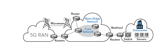
Figure 1 Optical modules are used from the 5G radio access network through the core network to the datacenter.
JITTER LIMITS DATA RATE
Optical modules convert optical signals into electrical signals and transform electrical signals into the optical format (see Figure 2). To avoid introducing errors into the data, the conversion poses a complex challenge to synchronize two time domains: the optical network with the electronics chipset. Synchronization is critical, and the component responsible for synchronizing the timing—aptly named the retimer—requires a reference clock with low jitter. The phase jitter in the retimer adds to the jitter in the serial data stream passing through the module, resulting in data errors if the jitter is too large. This becomes increasingly important as the data rates increase from 100 to 400 to 800 Gbps. As the throughput doubles from 400 to 800 Gbps, the jitter should reduce by 2x to maintain the same timing margin.
The RMS phase jitter of the oscillator quantifies the variation of a clock edge, and it is typically computed by integrating the phase noise across a 12 kHz to 20 MHz offset frequency range. For example, a differential oscillator based on MEMS technology from SiTime has a phase noise of -89 dBc/Hz close in, dropping to a noise floor of -170 dBc/Hz. Integrated across a 12 kHz to 20 MHz offset from a 156.25 MHz clock yields an RMS phase jitter of 70 fs.
Another important factor determining oscillator performance is the presence of spurious signals, which will increase the jitter. Figure 3 compares the phase noise responses of MEMS and phase-locked quartz oscillators. While the phase noise of the two appear comparable, the phase-locked quartz oscillator (Figure 3b) has several spurs, which increase the phase jitter to 267 fs, compared to 70 fs for the MEMS oscillator. Without the spurs, the RMS phase jitter of the quartz oscillator would be 90 fs, meaning the spurs contribute 66 percent of the total jitter. The MEMS oscillator uses an integer-N PLL architecture to avoid spurs and minimize the phase noise.
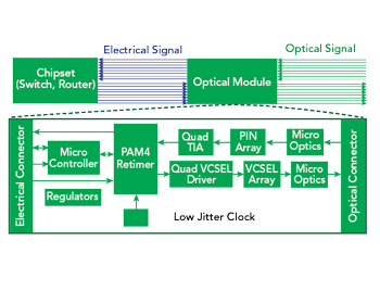
Figure 2 Optical module block diagram. The jitter of the clock limits the performance of the retimer.
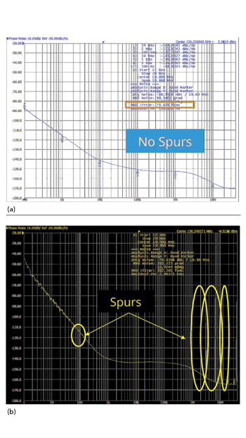
Figure 3 Phase noise and spur performance of MEMS-based (a) and phase-locked loop quartz (b) oscillators.
MINIMIZING SIZE
While the optical modules are increasing their data rates by 2x to 4x, the components used in the modules must support these higher data rates without significantly increasing circuit board footprint or power consumption. Reducing the footprint of the retimer is important because more than half of the optical module is used by the laser subassembly and its electronics, which leaves little room for the signal processing circuitry.
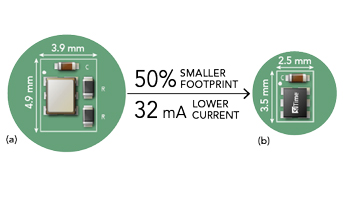
Figure 4 Size and current consumption of AC-coupled LVPECL oscillator (a) and MEMS-based oscillator with integrated LVPECL source-bias resistors (b).
Comparing the MEMS and quartz oscillators, the MEMS oscillator has a 2.0 × 1.6 mm footprint compared to 2.5 × 2.0 mm for this quartz oscillator (see Figure 4). The MEMS oscillator includes on-chip voltage regulators to filter power supply noise, which saves board area and improves the power integrity in the module. By integrating two source-bias resisters and using an AC-coupled output, the MEMS design reduced its footprint by 50 percent and current consumption by 32 mA. The MEMS oscillator design enables custom programming of the differential voltage swing at the factory so it can comply with the differential input swing of any chipset, including low voltage chipsets with nonstandard voltage swings. By matching the needs of the chipset, the typical termination can be eliminated, which reduces current to 16 mA with a DC-coupled LVPECL output.
SUMMARY
The evolution of the optical network to 400 and 800 Gbps data rates demands improved optical module performance without increasing size and current consumption, requiring the oscillator in the module to provide low jitter while minimizing power consumption and footprint. With innovations such as integrated bias resistors and programmable voltage swing, MEMS-based differential oscillators reduce the footprint and current consumption while achieving 70 fs RMS phase jitter. MEMS oscillators provide a timing solution that meets the needs of optical modules for 5G networks.