It is possible in certain instances to improve the performance of a design that uses a MMIC low noise amplifier (LNA), using the same concepts for discrete transistor LNA designs. In this article, a design using a MMIC LNA is optimized over a 5G frequency band to achieve a lower noise figure than specified on the device datasheet.
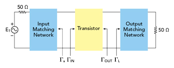
Figure 1 Single stage LNA topology.
An LNA is a critical component typically found in any receiver chain. Its purpose is to amplify an extremely weak signal captured by the receiver’s antenna, adding minimal noise power to the signal. An LNA’s noise figure is an important parameter enabling a designer to determine whether a given LNA is suitable for a requirement. Noise figure is the decibel representation of noise factor, a measure of the degradation in the signal-to-noise ratio as a signal passes through a network. LNAs are available as MMICs from various manufacturers, and it is often possible to purchase a MMIC LNA with the performance needed for a requirement, rather than having to design an LNA using a discrete transistor. The MMIC LNA can then be incorporated into the overall design by mounting it on a printed circuit board, following the manufacturer’s instructions. In contrast, designing an LNA with a discrete transistor generally requires more effort than using a MMIC because discrete transistor LNA design involves creating appropriate matching networks so the amplifier achieves the desired performance.
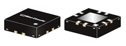
Figure 2 PMA-5451+ MMIC LNA.
To illustrate, Figure 1 shows a single-stage amplifier design consisting of an input matching network, a transistor and output matching network. The minimum noise figure is achieved when the source reflection coefficient (ΓS) is properly selected; the value of ΓS achieving the minimum noise figure is known as Γopt. Γopt, with the minimum noise figure, Fmin, and the equivalent normalized noise resistance, rn, are provided by the manufacturer of the transistor or can be determined experimentally.1 In general, the goal when designing an LNA with a discrete transistor is to design the input matching network to achieve the lowest noise figure from the transistor and design the output matching network to help the LNA meet the requirements for output return loss, gain, gain flatness and other parameters.1,2
Compared to a discrete transistor LNA design, purchasing a MMIC LNA internally matched to 50 Ω seems easier because there is no need to design any matching networks. Instead, the MMIC is simply inserted into a 50 Ω environment following the manufacturer’s instructions, which is obviously quicker and acceptable in many cases. However, it may be possible to optimize the performance of the MMIC LNA by exploiting the same concepts used for a discrete transistor LNA design. A MMIC LNA may be specified to operate over a wide frequency range, and many designers may assume the noise figure in the datasheet is the best that can be achieved; however, a MMIC LNA may achieve a lower noise figure than shown in the datasheet over a portion of the frequency band. This improved performance can be achieved by optimizing the design over the desired frequency range.
In this article, we optimized an LNA over a 5G band using the PMA-5451+ wideband MMIC LNA from Mini-Circuits. The design was simulated using Keysight Technologies’ Advanced Design System (ADS) software. Modelithics models for the MMIC LNA and all passive components were used, and the Modelithics model for the PMA-5451+ was validated for both S-parameters and noise parameters, which were used to optimize the complete design for the best noise figure over the desired frequency band. The goal was for the noise figure of the optimized LNA to be lower than the typical noise figure for the PMA-5451+ specified in the Mini-Circuits datasheet. Measured data confirmed this approach.
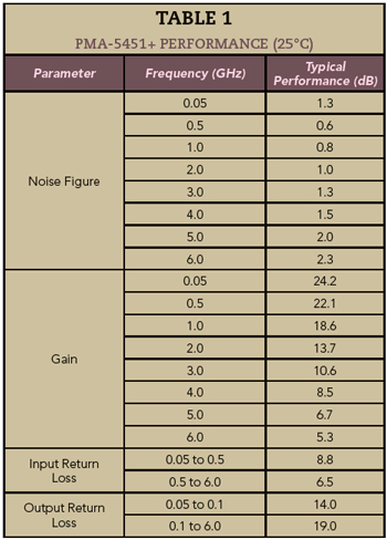
MMIC LNA PERFORMANCE
The Mini-Circuits PMA-5451+ MMIC LNA (see Figure 2) is fabricated using an enhancement-mode PHEMT process. The operating frequency range is specified from 50 MHz to 6 GHz. Operating from a single +3 V DC power supply, the MMIC typically draws 30 mA with a 1.5 kΩ bias resistor. It is assembled in a 3 × 3 mm package. The PMA-5451+ data sheet contains a schematic of the recommended application circuit (see Figure 3) and the characterization test circuit used to determine device specifications. The typical gain, noise figure and input/output return loss at +25°C are shown in Table 1. The table shows the PMA-5451+ has typical noise figures of 1.3 and 1.5 dB at 3 and 4 GHz, respectively. For this design, the goal is to minimize the noise figure from 3.3 to 3.8 GHz, which is the n78 5G NR band.
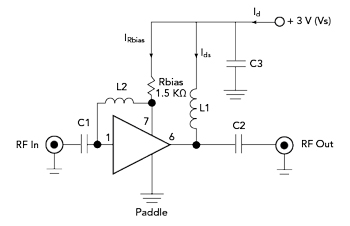
Figure 3 PMA-5451+ application circuit.