

As the industry shifts toward higher speed designs and next-generation wireless communications, insertion loss and the ability to predict it have become constraints to achieving higher speeds. While the industry has been working on increasing data rates through new signaling techniques, loss modeling leaves much to be desired, requiring multiple revisions of signal integrity (SI) test vehicles - a very expensive and time-consuming process that may take many months before completing loss validation. Another pain point is caused by the increasing number of inputs and outputs on devices, yet miniaturizing circuits to be compact. As such, dimensional deformation, coefficients of thermal expansion (CTE) and the moduli play major roles in determining manufacturability and reliability. Products designed solely for optimizing SI may suffer from unintended poor reliability, costing major delays in time to market.
Recognizing this, Avishtech has built tools to help solve these challenges in an integrated, multidisciplinary fashion - not in silos. Avishtech has released two products: Gauss 2D, to address SI issues, and Gauss Stack, for the thermomechanical, manufacturability and reliability concerns.
Gauss 2D is an electromagnetic (EM) field solver that goes beyond other offerings by providing extremely high accuracy and granularity, coupled with additional features. Gauss 2D provides more than basic impedance information for a printed circuit board (PCB) transmission line:
- Detailed loss information, including accurate conductor loss to account for the proximity effect
- Full RLGC parameters, including matrices for multiconductor configurations
- Frequency-dependent modeling and projection of these properties, including frequency-dependent S-parameters (see Figure 1)
- Crosstalk calculations for differential and multiconductor configurations
- Dielectric property extraction
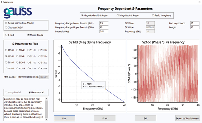
Figure 1 Gauss 2D S-parameter interface, showing a 10 in. long differential stripline.
Gauss 2D also provides visualization of the electric potentials and fields, giving deeper granularity and further insight into concerns like coupling and interference (see Figure 2). The ability to predict losses accurately helps avoid multiple iterations of test vehicles on different material sets and different copper types.
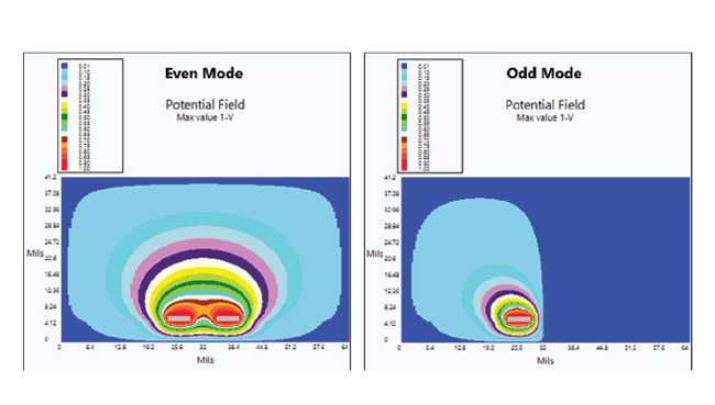
Figure 2 Electric potentials for even and odd modes of a differential microstrip trace.
Gauss Stack is the industry’s first and only complete simulation environment for PCB stackups, enabling users to rapidly design a stackup and conduct high fidelity thermomechanical and electromagnetic simulations. The thermomechanical simulations address dimensional stability and reliability, among other issues. Gauss Stack is the only tool that predicts dimensional movement for the grain and fill directions for each core layer in a stackup. Anyone who has worked in a PCB shop can attest that manufacturing PCBs is a complex process, in part from iterating through compensation factors to achieve successful circuit registration between layers. Gauss Stack’s highly accurate predictions enable a board shop to bypass this expensive and lengthy process of compensating through scout lots and databases. Boards can be built correctly the first time - a key enabler of quick-turn capabilities benefiting both board shops and customers, as well as improving yield.
Figure 3 compares the predictions from Gauss Stack with measurements of test vehicle boards. The bars in the plots show a 150 ppm range around Gauss Stack’s predictions, which includes all the measured data. The overwhelming majority of the data points are within a small fraction of the 150 ppm bounds. This confirms aggressive registration targets can be met using Gauss Stack’s predictions, eliminating scout lots.
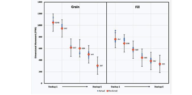
Figure 3 Gauss Stack predictions vs. measurements of test vehicle boards. The bars represent 150 ppm from the Gauss Stack predictions and contain all the measurements.
With Gauss 2D, simulation is easy using its extensive set of predefined geometric configurations with detailed information and accuracy - literally seconds to set up a problem. These include the traditional microstrip and stripline configurations, as well as coplanar waveguide, multiconductor and dual dielectric configurations. Gauss 2D accounts for dielectric anisotropy, which enables the user to input Dk and DF properties in both perpendicular and parallel directions. Gauss 2D can also synthesize, enabling a user to “flip the problem,” i.e., obtain the trace width corresponding to a target impedance. This capability is built on a nonlinear Newton solver that searches for the desired field solver solution.
Reliability is a critical consideration in PCB design. From an SI standpoint, many “ideal” PCB designs can have low reliability, due to high stresses or significant mismatches in material properties. An extremely low loss design with perfect SI behavior means nothing if the board fails during assembly. Gauss Stack enables designers to obtain key board properties in all three dimensions: CTE, elastic and shear moduli and Poisson’s ratios, all at board level. These properties cannot be calculated by any other tool, and they are the primary inputs - with or without a separate CAD model - for granular reliability simulations of cycles to failure. Gauss Stack calculates X and Y stresses for each material layer, providing insight into the reliability of a design and the impact of changing resin content, glass style, number of plies and other stackup parameters.
To illustrate, the screenshot in Figure 4 shows the material properties for a chosen resin system in a stackup (on the left), with Gauss Stack’s thermomechanical outputs (on the right). These outputs enable reliability simulation by accurately accounting for the bulk properties of the PCB. In addition to the comprehensive thermomechanical data, the built-in Gauss 2D engine calculates impedance and can synthesize the entire stackup - up to three single-ended and three differential traces per signal layer. All the transmission lines for an entire stackup can be designed with a single click after specifying the target impedances. This paired with Gauss Stack’s extensive vendor-specific materials library make designing a PCB stackup a breeze.

Figure 4 Material properties for a resin system used in a stack (left) and Gauss Stack thermomechanical outputs (right).
The Gauss suite of products provides deep insights not available with other simulation programs, combining extreme accuracy with ease-of-use. As important, Gauss 2D and Gauss Stack enhance design productivity by reducing complex steps - which can take days, weeks or longer - to simple tasks that take just minutes. The result: reduced time, cost and risk.
Avishtech, LLC
San Jose, Calif.
www.avishtech.com