

THEORY OF OPERATION
Important in the design of a multi section tunable filter is to use a structure that maintains a desired filter response over the full tuning range while varying as few component values as possible. This filter is a 4-pole lumped element bandpass design that varies the inductor value associated with each pole to tune the center frequency of the filter.
The filter schematic is shown in Figure 4. This topology provides inherently good harmonic rejection due to the large number of shunt capacitors. The “pi” sections of capacitors between each inductor have a constant ratio of reactance between each other as frequency is varied. This allows the response of the filter to be maintained over a wide frequency range. As only the inductor values are varied and the capacitor values remain constant, percentage bandwidth is constant with frequency. This means that filter bandwidth increases with increasing frequency which is generally desirable as insertion loss and harmonic rejection then stay constant.
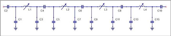
Figure 4 Filter schematic.
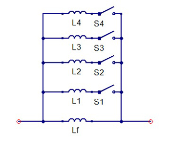
Figure 5 Switched inductors.
Variable inductors are realized by means of fixed inductors that are switched in and out of the circuit using MEMS switches (see Figure 5). Switches S1 thru S4 are the arms of an SP4T MEMS switch. Each arm may be controlled independently providing a total of 16 possible switching states. Inductors L1 through L4 are switched in parallel with the fixed inductor Lf, effectively lowering the overall inductor value. At high frequencies, where minimum inductance is required, most of the switches are closed, which reduces the ON resistance of the switch as multiple paths are closed in parallel.
The MEMS switch is an ideal element for this type of application as it has both very low on resistance (<0.5 Ω) and off capacitance (0.03 pF) which means any parasitic resonances appear well out of the band of operation. When compared to other solid-state switch technologies, these have very low parasitics.
The MEMS switches are activated via electrostatic force, and thus require a high voltage source for switching. The gate of the switch is set for a bias of 0 VDC, which places the metal cantilever beam in a non-deflected (off) state. Thus, the path between the RF input and output is isolated with an air gap, like a traditional mechanical relay. When the gate is set to its actuation voltage of +88 V, the electrostatic force between the gate and cantilever beam is strong enough to cause it to deflect downward, forming a connection with the contact and closing the switch (on state). Given the low supply current necessary for electrostatic operation, a single charge pump circuit is used to generate the +88 V required by each of the sixteen (4 x SP4T) MEMS switches.
LAYOUT
The filter circuit is very tolerant of layout due to the large number of shunt capacitors that can be incorporated into PCB traces, providing design flexibility. One critical area, however, is the connection between the inductors and the switch where it is important to minimize any stray capacitance that may form a parasitic resonance when combined with the lumped inductor. For this reason, the switched inductors are grouped closely around each individual switch with trace lengths and widths as small as practical.
SMALL-SIGNAL PERFORMANCE
Measured S21 for the seven filter steps is shown in Figure 6, while Figure 7 shows |S21| and |S11| for Channel 3. The filter response has good selectivity and the insertion loss is constant over the tuning range. The MEMS switch works very well for this application and insertion loss is dominated by the finite Q factor of the inductors, capacitors and PCB material. Note the consistency of insertion loss as the frequency is tuned across the band of interest.
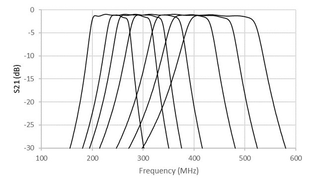
Figure 6 |S21| for the seven frequencies of the tunable filter.
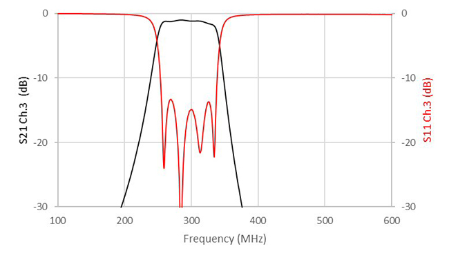
Figure 7 |S21| and |S11| for Channel 3 (250-340 MHz) of the tunable filter.
POWER HANDLING AND THERMAL PERFORMANCE
The MEMS switch selected for this filter exhibits a very low insertion loss of 0.15 dB at 4 GHz as well as third-order intercept greater than 85 dBm, while capable of handling 25 W of RF input power in a 50 Ω system. In addition, it is designed to handle up to 160 V without damage, which allows it to be used safely in the resonant element of a filter. In this filter design, care is taken to use a relatively low internal impedance. Figure 8 shows the maximum voltage gain relative to 50 Ω seen by the switches. Within the filter passband, this voltage gain reaches a maximum of 3 ensuring that at higher power operation peak voltages are relatively low. When approaching CW input power levels of 60 W, however, the switches still must handle greater than 100 V. This can be problematic for most solid-state technologies which must resort to transistor stacking, which degrades switch parasitics.
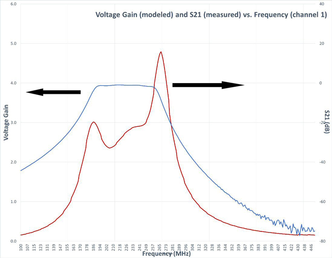
Figure 8 Peak voltage gain seen by switch element relative to 50 Ω input.
The low loss and high voltage handling capability of the MEMS switch translates to significant gains in power density and thermal performance for the filter. Compared with the switched filter bank which may have as much as 3 dB additional insertion loss, the input power requirements for a given output level are significantly reduced which has additional benefits with respect to power dissipation.
Compared with varactor tuned filters, switches have much better linearity and power handling for tunable applications. The only limitation is the number of discrete tuning states available. Solid-state switches do not have the same combination of almost zero power consumption and high IP3 exhibited by the MEMS switch. This makes the MEMS switch an ideal candidate for use in discrete tunable filters.
The filter’s thermal profile when tested up to 35 Watts CW (test set limitation) is shown in Figure 9. As expected, the majority the filter’s power dissipation is in the inductors.
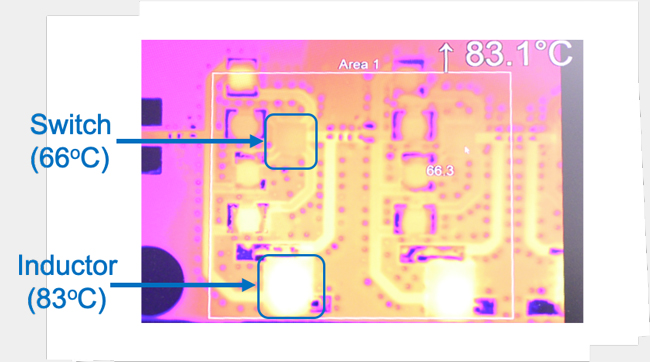
Figure 9 Filter thermal profile.
Small-signal testing over temperature is shown in Figure 10. The elimination of solid-state devices from the filter helps to significantly improve the insertion loss stability over temperature.
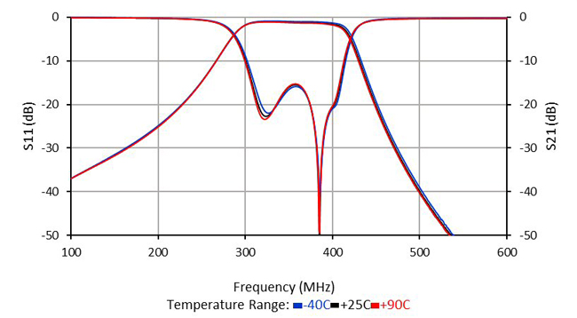
Figure 10 Filter performance over temperature.
CONCLUSION
The enhanced performance of this miniaturized tunable filter is attributable to the switch’s unique technology. The very low levels of parasitic off capacitance and very low on resistance result in a high Q resonator that replaces multistage solid-state components and associated biasing circuitry, reducing the filter’s size and weight. Since the switches are inherently low loss, this filter design can handle much higher power levels with lower heat dissipation than a traditional switched filter bank. These are advantages that also reduce total cost of the filter while allowing it to meet the stringent requirements for emerging multiband radio systems.
By more closely integrating the switch and inductor combination to minimize parasitic capacitance, the frequency range can be extended up to 6 GHz with existing switch topologies. This enables improvements over existing filter technologies, especially for the emerging 5G sub-6 GHz NR RF infrastructure.
As the ON resistance of the switch is very low, the frequency of operation can easily be extended down into the HF/ VHF band without the necessity of using large value inductors as the frequency reduction can mostly be achieved by increasing shunt capacitor values. This allows air cored (non-ferrite) inductors to be used at much lower frequencies, which minimizes size and improves stability and linearity. This same property facilitates the realization of more sophisticated filters with greater selectivity to maximize rejection close to the passband.
The use of additional switch arms allows more discrete steps to be implemented, further approximating a continuously tuned filter. This allows filter bandwidth to be reduced as the switching circuits are not a significant contributor to the overall insertion loss. A practical limit is in the region of 6 bit control giving a total of 64 discrete frequencies. In addition, using more switches to select multiple tunable resonators allows more frequency bands without significant sacrifices in overall insertion loss and size.

For more on this topic, watch Menlo Micro's webinar: Innovative Approaches to RF Filter Design Using High Power MEMS Switches