
While Figure 6 shows the predistorter’s action on out-of-band spectral emissions, Figure 7 illustrates the concurrent improvement of in-band distortion that results from linearization. The figure shows the transmitted constellation for a 64 QAM carrier before and after linearization. The predistorter removes the AM-to-AM and AM-to-PM distortion introduced by the PA which would otherwise increase the modulation error as shown in Figure 7a. For this example the modulation error ratio is improved by approximately 6 dB.
While DPD enhances power efficiency, the linearizer subsystem does of course consume additional power associated with the correction engine, adaptation processing, enhanced forward path bandwidth and feedback path. The power consumed by the predistortion system varies significantly according to the transmission standard, target technology and performance level sought; though, for wideband 4G/5G applications a very rough estimate might be 3 W. For lower transmit power applications such as small cell and MIMO this figure should be established to confirm that predistortion provides a net efficiency improvement (assuming DPD is not mandated by other considerations such as spectral emissions compliance).
FEEDBACK PATH
An unavoidable fact in predistorter design is that the linearity of the feedback path represents a limit on available performance. Because the feedback path falls within the control loop, the predistorter introduces a correction signal for the feedback path nonlinearity, which in turn is imposed upon the transmit output. During hardware design careful attention to feedback path linearity, including that of the data converter is required to ensure it does not compromise performance. In contrast to a conventional receiver design the feedback receiver path linearity tends to be a more important consideration than SNR.
Similar considerations apply to any linear feedback path distortion such as gain and phase variation which may be superimposed on the transmit path if not addressed. Digital linear equalization of the feedback path can be used to mitigate this effect, though characterizing the response of the feedback receiver in isolation can be tricky.
It is a common misconception that the feedback path bandwidth should be equivalent to the forward path correction bandwidth. In fact, the design requirement is that the feedback path should span sufficient distortion orders to facilitate construction of the forward path correction signal, which may be less than the forward path bandwidth. Figure 8 shows two waveforms, both with the same instantaneous bandwidth. The image in Figure 8a comprises two narrow-band carriers and it is apparent that the third and fifth order distortion products occur at discreet locations. To capture IMD5 information, the feedback path must be 5x the instantaneous bandwidth. In this case it is necessary for the feedback bandwidth to equal that of the forward path.
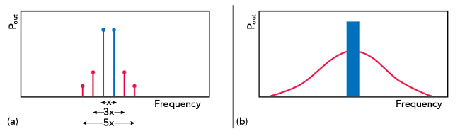
Figure 8 Two-tone (a) and wideband (b) intermodulation distortion spectra.
Now consider Figure 8b showing a wideband noise-like carrier with distortion products that are diffuse, falling both within and outside of the modulation bandwidth. If a feedback bandwidth of less than 5x the modulation bandwidth is employed it will still capture a proportion of IMD5 (and higher) products. For this scenario it may be possible to use a feedback bandwidth less than that of the forward path. In practice the feedback path bandwidth should be designed empirically as restricted bandwidths can reduce algorithmic convergence time, which may or may not be a consideration.
PERFORMANCE OPTIMIZATION
To obtain optimum performance from a digital predistorter, it is necessary to account for and address hardware deficiencies and non-idealities (in addition to the PA nonlinearity) that would otherwise degrade the correction level achieved. Non-flat gain and phase slopes across the analog forward and feedback paths, local oscillator phase noise, direct conversion gain and phase imbalance, carrier leakage, PA gain variation and control loop timing variability can all degrade performance. The more sophisticated DPD solutions incorporate subsystems to correct the majority, if not all these non-ideal characteristics. Indeed, one of the greatest challenges to successful predistorter design is to orchestrate the operation of these correction subsystems to avoid adverse interaction between them and to allow the primary nonlinear correction engine to be deployed solely against the PA nonlinearity.
Worthy of specific mention are amplifier memory effects, where the PA output is a function of current input signal and its past history. Sources of memory effect are numerous and include:2
- Gain variation with frequency across the modulation bandwidth.
- Transistor power supply variations (e.g. non-deal response of the drain circuitry at the modulation frequency).
- Thermal effects whereby device junction temperature changes modify the nonlinear characteristic at the modulation envelope frequency.
- Charge trapping effects. All semiconductor materials and interfaces tend to capture and later emit charge (holes and electrons) within the transistor channel, causing changes in current flow that are dependent upon not only the instantaneous device voltage but also the history of the voltage signal. Of relevance to 5G is the increasing popularity of gallium nitride (GaN) transistors for wideband transmission. Compound semiconductors such as gallium arsenide (GaAs) and GaN have greater susceptibility to charge trapping than conventional silicon laterally diffused metal oxide semiconductor transistor.
Linearized performance is substantially degraded if the hardware exhibits memory effects that exceed the correction capability of the DPD. This is an area where scalable (field-programmable gate array (FPGA)-based) DPD has an advantage as there is the potential to increase the complexity of the correction engine to accommodate the PA’s memory depth. This does, however, consume additional signal processing resources and designing PAs to minimize memory effect is the preferred approach, where feasible.
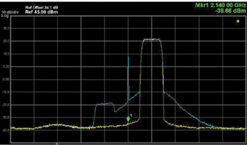
Figure 9 Suppression of the carrier image and LO using DPD.
Figure 9 illustrates the operation of a correction subsystem in the form of a predistorter with the capability to automatically suppress the carrier image from the gain and phase imbalance of the analog quadrature modulator (AQM) of a direct conversion transmitter. It is apparent that the correction algorithm also has the capability to suppress the local oscillator (LO) leakage of the AQM to a high level. The best DPD systems have the capability to independently correct carrier images and LO leakage associated with the forward and observation paths, thereby preventing the observation path correction signal from being imposed upon the transmit output.
Care is required when positioning ancillary digital correction engines within the forward path as the nonlinear nature of the system means that superposition may not apply. For example, the above compensator intended to address AQM deficiencies should be located after the predistorter, and not before, to ensure that the compensated correction signal is not subject to a nonlinearity.
A sophisticated, latest generation predistorter can provide system benefits beyond linearization by virtue of the control loop formed by the feedback path. In addition to the above examples of linear equalization, carrier image and LO suppression, the DPD may also integrate compensation for PA gain variation with temperature. Furthermore, in multi-transmitter applications, such as beamforming or MIMO it is possible to commutate a common feedback path between the predistorter associated with each transmit chain and thereby achieve gain and phase alignment between channels.
CREST FACTOR REDUCTION
Crest factor reduction (CFR), like DPD, is a technology that can be used to enhance PA efficiency. It is, therefore, worth a brief summary here. CFR modifies the input signal to reduce its peak-to-average power ratio (PAPR), trading a reduction in signal peak power level for increased in-band modulation error (within system requirements). Since a PA is defined by its peak power handling capability, this enables operation at a higher mean power level for improved efficiency. CFR invariably requires a knowledge of the underlying transmission standard and carrier configuration.
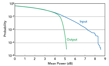
Figure 10 CCDF of a 64-QAM signal (input) showing CFR (output) to achieve 5 dB PAPR at 10-5 probability.
The capability of CFR is illustrated in Figure 10, which shows the simulated complementary cumulative distribution function for a 64 QAM satellite bearer where the CFR has been configured to provide 5 dB PAPR at 10-5 probability. Modern, noise-like linear modulations can have a very high PAPR for which CFR can provide peak reductions in excess of 5 dB for significantly enhanced efficiency.
In contrast, DPD improves efficiency by providing a level of PA linearity that would otherwise require the PA to be significantly backed-off or over-specified, with associated implications for transistor size and cost. DPD is more indifferent to the underlying modulation than CFR and derives a correction signal from the characteristics of the composite signal applied without a knowledge of the specific transmission standard. CFR and DPD are separate yet complementary technologies and may be used together or individually.
SUMMARY
It is important to appreciate that DPD system design is a co-design exercise between the predistorter (CFR, if employed), radio platform and in particular, the PA. While the latest generation DPDs are cable of correcting complex nonlinearities and hardware deficiencies, this consumes digital resources (FPGA or ASIC memory, registers and multipliers) which may be at a premium. Hence maintaining PA characteristics such as memory effect within the correction capabilities of the predistorter is desirable. PA saturation at the maximum anticipated signal drive level should also be avoided as no amount of signal expansion within the predistorter can compensate for a saturated nonlinearity. The PA need not be linear, but it should be designed to handle the input peak power, which will be dictated by the CFR, if used. The best outcomes are achieved when a PA is designed to be linearizable (i.e. system designed), rather than attempting to apply the technology to an arbitrary amplifier.
References
- S. Cripps, “Advanced Techniques in RF Power Amplifier Design,” Artech House, 2002, pp. 153-162.
- 2. J. Vuolevi and T. Rahkonen, “Distortion in RF Amplifiers,” Artech House, 2003, pp. 43-68.