
The onset of GaN as a semiconductor material is enabling the next generation of electronic devices. Because GaN is a wideband gap (WBG) semiconductor material, it can sustain higher breakdown electric fields and electron drift velocities than conventional semiconductors such as Si and GaAs.1 GaN also exhibits enhanced thermal characteristics, sustaining higher temperatures and more effectively conducting heat. Because of these desirable material properties, GaN devices can operate at higher frequencies and higher powers in smaller package sizes, an enabling development in the field of high-power semiconductors.
SOLID-STATE POWER AMPLIFIERS
GaN has great promise to revolutionize solid-state power amplifiers (SSPA) for space applications. GaN is a particularly good fit in space applications due to its small size, light weight and radiation tolerance from enhanced atomic bond strength. In traditional satellite architectures, amplifying a signal for transmission has typically been achieved either by using travelling wave tube (TWT) amplifiers, which are relatively large in size and weight, or lower power GaAs SSPAs, which require numerous units and additional signal combining hardware. With costs still near $10,000 per pound to get into low Earth orbit (LEO),2 the ability to shrink from ~150 in3 TWT amplifiers to operationally equivalent ~0.05 in3 GaN high-power amplifiers (HPA) will result in significant cost reductions as well as payload capability enhancements.
The byproduct, however, of shrinking the power amplifier to a package smaller than a penny is the increased power density. In SSPAs, device temperatures spike to very high local values at the microscopic gate fingers as power density increases, making the removal of heat a far more difficult task. Moreover, with an Arrhenius relationship between device mean time to failure (MTTF) and operating temperature, small changes in the device temperature can result in orders of magnitude differences in lifetime.3 It is therefore critical in high value, low-maintenance space payloads to have a reliable and effective cooling technique compatible with the shrinking package sizes and increasing power densities of GaN HPAs.
With current power densities of HPAs on space payloads eclipsing 50 W/cm2, traditional heat spreading cooling methods are reaching their limits. Moreover, with the enhanced material properties of GaN devices, power densities over 1500 W/cm2 are imminent in space payloads which is almost two orders of magnitude higher than those supported using standard thermal architectures. Therefore, a fundamentally different approach to thermal management is needed to fully capture the exceptional capabilities of GaN semiconductor devices while maintaining temperatures compatible with long-term, reliable operation on space platforms.
FUNDAMENTAL HEAT TRANSFER CONSIDERATIONS

Figure 1 Radiative cooling flux as a function of surface temperature, applying best case scenario of a 3 K cold sky with perfect emissivity and view factor.
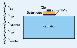
Figure 2 Schematic of conductive heat spreading thermal stackup. The heat generated in the die passes through multiple layers of interface materials and heat spreaders before reaching the radiator (not to scale).
Radiation heat transfer, assuming a perfect view factor to the surrounding cold sky, is governed by the Stefan-Boltzmann Law:

where q˙rad is the radiative cooling flux (W/cm2) from a surface of emissivity ε with temperature TH (K), radiating to surrounding cold sky temperature TC (K) often taken to be around 3 K. The Stefan-Boltzmann constant, σ, is a physical constant of proportionality denoting the total radiative transfer of a black body over all wavelengths, which takes the value
