
Ultra-wideband microstrip filters fabricated with precision techniques on alumina substrates operate in three different frequency bands, ranging from 20 to 56 GHz with fractional bandwidths exceeding 33 percent. The filters are designed for a frequency multiplier-based signal generator used in a compact ultra-wideband radar system. The first-pass computer-aided development process includes a sensitivity analysis to account for manufacturing tolerances, enabling the production of fully functional circuits on an accelerated schedule. The filters provide excellent electrical performance, as well as small size, low cost and ease of integration.
Compact microwave and mmWave filters with fractional bandwidths exceeding 20 percent are in demand for applications such as wireless communications and radar. Microstrip bandpass designs implemented using high permittivity ceramic substrates have been widely reported;1-3 however, some disadvantages of these earlier realizations include significant insertion loss, narrow bandwidth and limited selectivity.4-8
To overcome a lack of acceptable commercial off-the-shelf filters with very specific passband and selectivity requirements in an accelerated development schedule, custom planar microstrip filters on alumina with fractional bandwidths exceeding 33 percent are produced with rapid prototyping. These ultra-wideband,9 low loss ceramic filters serve as preselect filters in a multistage frequency multiplier module used in the generation of highly linear frequency swept radar waveforms.
Figure 1 is a simplified block diagram of the frequency multiplier circuit, which uses a series of frequency doublers and two spectral translation stages to generate a wideband (2 to 18 GHz) chirp from a 0.1 to 1.1 GHz baseband signal.10 This work focuses on the blocks marked in red and labeled “alumina.” The blocks labeled “cavity” are tailored interdigital cavity bandpass filters.
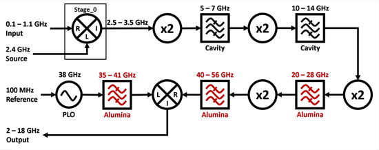
Figure 1 Simplified block diagram of the frequency multiplier-based waveform generator.
The output of each multiplier stage is filtered to reduce out-of-band harmonics. Wideband amplifiers, not included in the block diagram, are used to adequately drive succeeding stages. A pair of wideband mixers performs the required up- and down-conversions. The 2.4 GHz source pumping the up-conversion mixer (labeled “Stage_0”) and the 38 GHz oscillator used with the second mixer are phase-coherent. Similar circuits for generating radar ultra-wideband FM waveforms have been reported by Kocher,11 Li,12 Gomez-Garcia et al.13 and Yan et al.14 The primary advantages of the Figure 1 implementation versus prior designs are:
- Frequency selection is made so that harmonic content produced by the frequency multipliers is kept outside the bands of interest as much as possible.
- There is a sufficient guard band at each multiplication stage to minimize additive frequency roll-off and increasing group delay at the band edges.13
- This design is geared toward the implementation of a compact module suitable for operation on unmanned aerial vehicles.
This work focuses on the design, manufacture and characterization of the filters employed in the last three stages of the multiplier: two ultra-wideband designs covering the 20 to 28 and 40 to 56 GHz bands, respectively, and a 35 to 41 GHz design for the 38 GHz local oscillator (LO) signal from the last down-converter stage. The three circuit designs are simulated with electromagnetic analysis tools and fabricated by a commercial foundry. Multiple sets of measurements on the final products are compared with simulation, demonstrating first-pass success in the design process.
FILTER DESIGN FLOWThe filter chosen for the 20 to 28 GHz band is a fifth-order coupled-line Chebyshev design.15Once synthesized, a circuit simulator is used to define a parametric model enabling adjustment of the filter’s line widths (w1, w2 and w3), lengths (l1, l2 and l3) and separation between coupled lines (s1, s2 and s3). The line width of the input/output microstrip, designated w_50, as well as the coplanar waveguide feed dimensions are set for 50 Ω. The length of the microstrip line from the feed is made long enough to isolate the coupled-line section from the edges and to accommodate any mechanical structures that shield the filter in an integrated assembly. Optimization and tuning are performed to achieve the desired response. The filter is designed to pass the 20 to 28 GHz chirp from the third multiplier stage with small guard-bands on each side, to prevent operating in the region where group delay increases more rapidly and introduces phase distortion in the desired signal. Another design requirement is that third-order harmonics in the 30 to 42 GHz band from the preceding multiplier stage, whose input is a 10 to 14 GHz chirp signal, are suppressed along with the higher-order harmonics.
Three figures of merit are established as goals to optimize performance for each frequency multiplication stage:
(1) Stop-band attenuation of 20 dB at 2 GHz from the band edge.
(2) In-band insertion loss of less than 2 dB.
(3) In-band return loss better than 20 dB.
Multiple configurations supported by simulations are analyzed to achieve the best performance trade-off. For discrete optimization, geometric variables are defined with a step size of 2.54 μm (0.1 mil) and a minimum trace width of 12.7 μm (0.5 mil), as specified by the commercial foundry.16 The filters use a 127 μm (5-mil) thick alumina (Al2O3) substrate with a gold conductor; the dielectric constant is 9.9 and tanδ = 0.002. The conductor is sputtered with 2 μm of gold and metallized with TiW.
A genetic algorithm is used for optimization. The algorithm yields a new variable set after multiple iterations to minimize the cost function error. Dimensions are updated when the error is minimized and the solution appears to converge. A planar finite element circuit simulator is used to generate a more accurate filter model. The dimensions of the 20 to 28 GHz filter after optimization are shown in Figure 2. A similar process is followed for the 40 to 56 and 35 to 41 GHz filters, whose dimensions are shown in Figures 3 and 4, respectively. The passband of the 35 to 41 GHz filter is expanded to accommodate other frequency plans that may require a different LO frequency (e.g., 40 GHz).
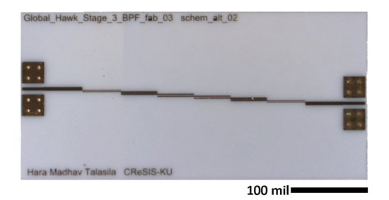

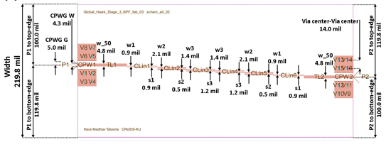
Figure 2 Top view of the fabricated 20 to 28 GHz filter (a) with parameters and dimensions in the x- (b) and y- (c) directions.

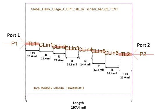
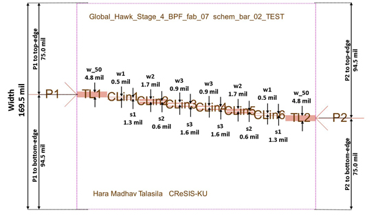
Figure 3 Top view of the fabricated 40 to 56 GHz filter (a) with parameters and dimensions in the x- (b) and y- (c) directions.
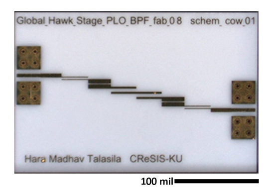
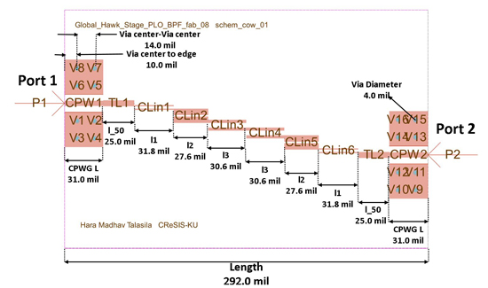
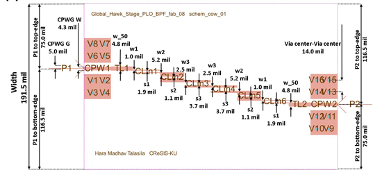
Figure 4 Top view of the fabricated 35 to 41 GHz filter (a) with parameters and dimensions in the x- (b) and y- (c) directions.
A sensitivity analysis accounts for fabrication tolerances and deviations by randomly sweeping the simulated design dimensions. Multiple sets of filters with frequency offsets in the response are used to check for potential shifts in the passband. Figure 5 shows the results of a sensitivity evaluation illustrating the effect of a 2.54 μm (0.1 mil) deviation from nominal design parameters. The target insertion loss, |S21|, is within acceptable limits, and the span of uncertainty is acceptable. Fabrication of the filter is feasible.

Figure 5 Sensitivity analysis for first-pass design of the 20 to 28 GHz filter.
Embedding coplanar waveguide (CPWG) feeds into the 20 to 28 and 35 to 41 GHz filter structures helps reduce interconnect reflections and provides a good transition for final integration; however, simulations reveal that the square grounding pad and its via hole have a negative effect in the 40 to 56 GHz filter response, manifested as a dip in insertion loss close to 52 GHz. To overcome this issue, a microstrip feed is used, with a commercial tapered coplanar waveguide (CPW) to microstrip transition for the 40 to 56 GHz filter.
Design trade-offs are made to satisfy the design rules of the commercial foundry. Specifically, gold (Au) is used as the conductor instead of copper (Cu), and the position of the via holes relative to the edges and their separation are adjusted. A summary of the dimensions for the three filters is provided in the Table 1 and the worst-case measured insertion loss and |S11| in Table 2.