
Broadband VNA Design
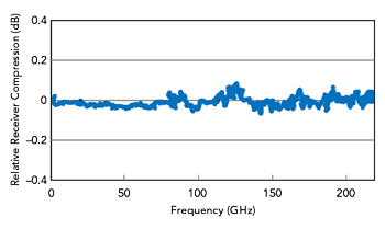
Figure 5 Relative compression of the VNA receiver, showing the difference between +5 and –20 dBm at the VNA port.
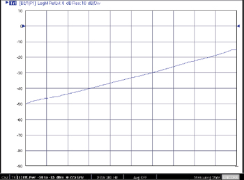
Figure 6 VNA power control range at 225 GHz.
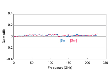
Figure 7 VNA stability over 24 hours at room temperature, measured using a thru-line.
One way to address these challenges is using a broadband VNA designed with high linearity receivers and sufficient integration and system control to ensure stability. The block diagram of one such system is shown in Figure 4a, comprising a base VNA and mmWave modules. The module receivers cover 30 to 226 GHz using broadband forward couplers and a high LO sampling system based on III-V nonlinear transmission lines.13 The port referred third-order intermodulation product of these down-converters exceeds 30 dBm, which helps meet the linearity requirements. The modules provide source multiplication above 54 GHz and use a series of four multiplexers, before the measurement couplers, to inject energy from the respective multipliers. Since progressively less power is available at the higher mmWave frequencies, the highest frequency multiplexer is last and has the tightest coupling. Leveling loops for both RF and LO extend to the modules to improve measurement stability.
The integration of the receivers, couplers and multipliers in a small space helps ensure thermal uniformity and stability, as does the close location of the couplers to the probe tip (see Figure 4b). The test port is a novel structure supporting a coaxial mode, using a 0.6 mm outer conductor and a precision UG-387 flange, instead of a threaded body, to form the outer mate. The increased mating area of the flange interface improves durability and significantly reduces the axial forces and bending moments of the connecting device. Repeatability with and without rotation is improved using a precision pin-guided UG-387 flange and limited angular connection orientations, 0 and 180 degrees. Such an interconnect system enables using a single on-wafer probe for measurements from 70 kHz to 226 GHz.
RF wafer probes convert the electromagnetic energy traveling along the three-dimensional media - a coaxial cable or rectangular waveguide - to the on-wafer DUT and its contact pads. This transition is designed to achieve minimal mismatch in the fields and impedance. This is particularly hard to achieve at sub-mmWave wavelengths, so precision wafer probe manufacturing processes are crucial to the overall system performance. Precision probes contribute to well-matched probes for improved calibration and measurement results over a wide frequency range. The 220 GHz MPI TITAN™ Probes incorporate 50 Ω MEMS contact tips to achieve the frequency coverage. Another important aspect of the probe design is maintaining visibility of the tip contacts during touchdowns to minimize potential inaccurate placement. Consistent positioning of the probes on calibration standards and small DUT pads achieves better repeatability and reproducibility, even when used by inexperienced operators. An often-overlooked aspect of probe technology is wear. After multiple probe cycles, the length of the probe tip typically shrinks. However, the unique design of the TITAN probe maintains the RF characteristics after hundreds of thousands of cycles; the lifetime of the probe outperforms the lifetime of comparable probe technologies - even on Al DUT pad metallization - reducing the cost of test and ROI of the test cell.
Using an external stimulus, Figure 5 shows the relative receiver compression at +5 dBm input power relative to a −20 dBm input. This performance is achieved through careful control of the LO waveforms used to drive the sampling down-converters.14 As discussed, power control is an important attribute for accurate measurements. One way to achieve it is with a heterodyne detection circuit feeding a leveling loop with widely adjustable time constants and gain. In this system, a wide control range of approximately 35 dB at 225 GHz (see Figure 6) and generally greater than 40 dB below 220 GHz is achieved with reasonable control linearity.
Stability is important to maximize the time between probe tip calibrations and avoid adding data distortion that complicates model fitting and analysis. Figure 7 shows the transmission measurement of a thru line in the port interface’s coaxial structure over 18 hours at 25°C ±3°C. As expected with temperature variation affecting LO cables, the drift increases with frequency since the LO multiplication factor increases with frequency. As the VNA receivers are used below 30 GHz, the RF cable to the modules (see Figure 4) contributes more at the lower frequency.
Summary
Increasingly, broadband mmWave VNA measurements are needed at higher frequencies, creating measurement challenges: stitching data from multiple bands, controlling power levels and ensuring linearity and stability. An integrated, broadband 220 GHz system with a single connection to the DUT is a simple and elegant approach to address these challenges. The linearity, power control, noise performance and stability of such a system improves measurement accuracy and repeatability.
References
- H. Chen, H. Zhang, S. Chung, J. Kuo and T. Wu, “Accurate Systematic Model-Parameter Extraction for On-Chip Spiral Inductors,” IEEE Trans. Elec. Dev., Vol. 55, November 2008, pp. 3267–3273.
- I. Angelov, K. Kanaya, S. Goto and M. Addasi, “On the High Frequency De-Embedding and Modeling of FET Devices,” 73rd ARFTG Conf. Dig., June 2009, pp. 1–4.
- C. Fager, L. J. P. Linner and J. C. Pedro, “Optimal Parameter Extraction and Uncertainty Estimation in Intrinsic FET Small-Signal Models,” IEEE Trans. Micr. Theory Techn., Vol. 50, December 2002, pp. 2797–2803.
- M. T. Yang, P. P. C. Ho, Y. J. Wang, T. J. Yeh and Y. T. Chia, ”Broadband Small-Signal Model and Parameter Extraction For Deep Sub-Micron MOSFETS Valid Up to 110 GHz,” 2003 RFIC Symp. Dig., June 2003, pp. 369–372.
- D. Williams, W. Zhao, R. A. Chamberlin, J. Cheron and M. Urteaga, “Verification of a foundry-Developed Transistor Model Including Measurement Uncertainty,” 87th ARFTG Conf. Dig., June 2016, pp. 1–4.
- J. Martens, “Parameter Extraction from 110+ GHz S-Parameter Measurements: A Heuristic Analysis of Sensitivity and Uncertainty Propagation,” 2011 COMCAS Conf. Dig., November 2011, pp. 1–4.
- D. F. Williams, A. C. Young and M. Urteaga, “A Prescription for Sub-Millimeter-Wave Transistor Characterization,” IEEE Transactions on Terahertz Science and Technology, Vol. 3, April 2013, pp. 433–439.
- N. Derrier, A. Rumiantsev and D. Celi, “State-of-the-Art and Future Perspectives in Calibration and De-Embedding Techniques for Characterization of Advanced Sige HBTs Featuring Sub-THz fT/fMAX,” IEEE Bipolar/BiCMOS Circuits and Technology Meeting (BCTM), 2012.
- D. F. Williams et al., “Calibration-Kit Design for Millimeter-Wave Silicon Integrated Circuits,” IEEE Trans. On Micr. Theory and Techn., Vol. 61, July 2013, pp. 2685–2694.
- X. Ye, “De-Embedding Errors Due to Inaccurate Test Fixture Characterization,” IEEE Electromagnetic Compatibility Mag., Vol. 1 No. 4, April 2012.
- J. Martens, “Common Adapter/Fixture Extraction Techniques: Sensitivities to Calibration Anomalies,” 74th ARFTG Conf. Dig., Dec. 2009, pp. 1–11.
- L. Galatro, S. Galbano, A. Santaniello and M. Spirito, “Power Control for S-Parameters and Large Signal Characterization at (Sub)-mmWave Frequencies,” 85th ARFTG Conf. Dig., June 2015, pp. 1–4.
- J. Martens, K. Noujeim and T. Roberts, “An Improved Stability Broadband/mmWave VNA Structure,” 77th ARFTG Conf. Dig., June 2011, pp. 1–4.
- J. Martens, “Sub-mmWave and THz frequency Conversion: LO Waveform Control and Sampling Technologies,” 8th ESA Workshop on Millimeter-Wave Technology and Applications, December 2018.