
As markets tap higher mmWave frequencies, device and subsystem modeling will follow. These efforts require even higher frequency measurements and equipment limitations that can hinder the development. In addition to standard S-parameters, other measurements such as gain compression, intermodulation distortion and frequency conversion may be needed across wide frequency ranges. Concatenating banded instrument data can work, yet the setup and calibration times become long and, since the uncertainty differs by band, stitching together data sets results in discontinuities.
A broadband vector network analyzer (VNA) covering low frequencies through 220 GHz, with accompanying probes, can resolve many of these measurement complications. Developing such a VNA requires multiplier arrays with adequate output power and control, down-converters with good noise performance and adequate linearity, source and receiver multiplexing that handles wide frequency ranges and a broadband connection enabling a single on-wafer measurement covering the entire frequency range. This article discusses these challenges and the technology options to create a broadband VNA with the required stability, noise, linearity and power performance.
Measurement Requirements
Broadband S-parameters and other microwave measurements are central to many model extraction procedures.1–6 In others, microwave data serves to generate the parasitic elements in the device models. In either case, the quality of the underlying measurement data is important to overall model performance and any descriptive analysis. Further stressing the need for measurement quality, de-embedding is typically necessary to get from the probe tips to the device or subsystem boundaries. Measurements are often required beyond purely small-signal and linear to include compression (AM/AM and AM/PM), harmonics, intermodulation distortion, adjacent channel power rejection and other parameters. Those quasi-linear or nonlinear quantities may be part of a complete nonlinear modeling effort or may be used for basic characterization. Some of these parameters may only be invoked at the subsystem level, with other measurements used at that stage, such as frequency conversion (gain and phase) and modulation distortion. What is common to all is the need to perform the analysis over a very broad frequency range, using an instrument whose own linearity does not dominate the measurement.
Measurement Challenges
Measurements above F-Band (90 to 140 GHz) face several challenges. A typical setup may consist of a broadband system operating to 110 or 125 GHz with banded waveguide modules for the higher frequencies (e.g., 110 to 170 and 170 to 260 GHz or 90 to 140 and 140 to 220 GHz). Mounting and demounting the modules and probes from the probe station - unless one is fortunate enough to have two or three equivalent probe stations - can yield measurement errors.
For broadband device model parameter extraction and IC performance verification, product and process design kit specifications require the same device under test (DUT) to be measured at multiple temperature points (usually five or more), meaning multiple touchdown cycles to the DUT contacts. DUT contact pads suitable for sub-mmWave probing are very small, since parasitic pad reactance increases with frequency. As small pads support only a few RF probe touchdown cycles, measuring the same DUT over the multiple bands covering the whole frequency range and all temperature points may be impossible. This limitation requires engineers to choose different DUTs for different temperatures or frequency bands, which increases uncertainty in the measured parameters and resulting models. A measurement system that reduces the number of touchdowns or enables one touchdown measurements over a wide frequency range will help.
Conventional VNA frequency extenders are sensitive to the measurement laboratory environment. Without multiple feedback control loops, the broadband measurement system characteristics of the remote module can drift faster than those of the base VNA. This leads to more frequent system recalibration, increasing the cumulative measurement cycle time. Frequent system reconfiguration and changeover, required for wide frequency range measurements, increase test cell downtime and risk damaging expensive system components, such as the wafer probes and VNA extenders. This increases the already expensive cost of test.
Data Integrity

Figure 1 Data stitching anomalies occur at measurement transitions between equipment setups.
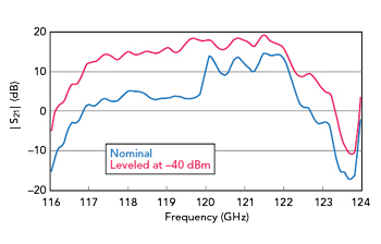
Figure 2 120 GHz LNA measured at two drive levels, where the nominal level compresses the amplifiers.
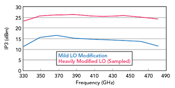
Figure 3 Third-order intercept point for two mmWave receivers with the same harmonic number but different LO designs.
Data integrity is also an issue. With several probes used for the different bands - each with unique touchdown characteristics, loss and matching - and several measurement modules used - with different matching, efficiency, spectral purity, stability and noise performance - the data in each band will be measured under different circumstances. While calibration corrects for some of these differences - however, not linearity, noise, spectral purity, drift or repeatability - the uncertainties and distributions in the bands will likely differ. This raises the question of how to handle the inevitable data steps (see Figure 1). The figure shows an example where the uncertainty ranges in two bands overlap; while nothing is fundamentally wrong with either measurement process, the discontinuity complicates the measurement and analysis. If the individual modules and probes have higher uncertainties at the band edges, the analysis becomes even more nuanced.7
Once the measurement data is collected, de-embedding to the desired reference plane can be an adventure. Particularly with BiCMOS and CMOS processes with five to nine metal layers, the desired transistor reference plane may be at the bottom layer and the probe pads at the top. This leads to a “network to de-embed” consisting of many vias and transitions, with significant insertion loss and mismatch.7–9 The increased loss and mismatch complicates the de-embedding process and increases potential error in the measurement results, particularly with drift.10–11 Since such semiconductor fabrication processes are increasingly used at mmWave frequencies, the stability and accuracy of the S-parameter data is critical, which emphasizes the challenges in stitching data and controlling uncertainties in all bands, including touchdown repeatability.
Ensuring Linearity
The RF drive level is important for transistors and amplifiers at these frequencies, as their input compression points may be low. The drive power may need to be −40 dBm or lower and accurate control of the power may be important to avoid inadvertent compression. For quasi-linear measurements, accurate power control is more important.12 The historic solution using a mechanical variable attenuator will not provide sufficient power flatness for this class of measurements. Figure 2 illustrates this, showing the measurement of a 120 GHz LNA where the drive level was not considered (the “nominal” curve). The input power to the LNA was not flat, reaching −15 dBm in places. A second measurement leveled the input power at −40 dBm. The nominal gain measurement shows the amplifier highly compressed, varying significantly with frequency because the drive was not flat versus frequency. While this example may be extreme, at higher mmWave frequencies - particularly with bare transistors - early onset compression is not unusual.
Even if the drive power is accurate, another challenge is the linearity of the instrument receiver; correcting for receiver distortion is difficult. Since many mmWave receivers use relatively high order harmonic mixing, the design of the internal local oscillator (LO) system is important to maintain linearity at the test port. A comparison of the intermodulation performance of two receivers is shown in Figure 3, using free space combining of two tones with 100 MHz separation. The two receivers have the same harmonic number but use different LO systems: one with mild clipping, the other more heavily clipped with active edge sharpening. The residual linearity, expressed as the third-order intercept point of the receiver referenced to the measurement plane, differed by close to 10 dB. As the converter designs have different breakdown voltages, broad conclusions are not possible; nonetheless, a wide variance in receiver linearity can occur in this frequency range.
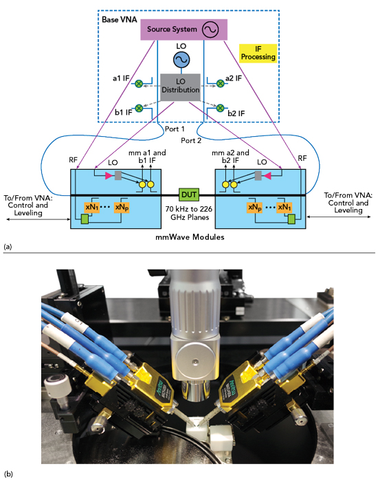
Figure 4 70 kHz to 226 GHz VNA block diagram (a), showing one measurement setup where the two mmWave modules are connected to on-wafer probes (b).