
The deployment of advanced 4G and 5G sub-6 GHz networks requires the introduction of new features and technologies by operators and phone makers. In order to provide access to the larger data bandwidth that the new network promises to deliver, the RF communication between the base station and user equipment must rely on a more complicated band setup. The complexity of the RF front-end module therefore increases dramatically and will have to integrate more than 100 filters to support all communication modes.
Different technologies are available to address the growing filter market but most struggle to meet the more stringent requirements demanded by the 5G networks. New Piezo-On-Insulator (POI) substrates, however, allow the manufacturing of high performance, integrated surface acoustic wave (SAW) filter components that can meet the requirements of 5G networks. These filters can be used in smartphone front-end modules along with the power amplifiers, switches and antenna tuners devices that are already manufactured using RF-SOI substrates or others.
5G Challenges of Front-End Modules
With 5G, larger RF spectrum provides access to data rates twenty times higher than 4G data rates. Devices connected simultaneously will multiply, resulting in a connection density of a thousand times higher than what is available today. All devices using the mobile network will be impacted by the arrival of this new standard.
To provide data rate in excess of 20 Gb/s, acoustic filters need to adapt to the complex challenges related to 5G networks: more bands, bands with larger bandwidths, higher frequency bands, many band combinations to support the different carrier aggregation (CA) modes and MIMO antenna design.
In order to achieve these new requirements, the signal selectivity needs to be more precise. For this, it is important to enable resonators that have an extremely low temperature coefficient factor (TCF), typically lower than 10 ppm/K, while providing a high Q-factor, Bode Q typically greater than 2000. Also, out of band rejection must be considered much more carefully in order to support the different carrier aggregation and MIMO features.
The optimization of energy consumption in the front-end module remains a key concern. The components must also limit insertion losses so that at equal power levels, the signal travel as far as possible and at the same time the device must dissipate the power very efficiently.
A proliferation of components inside the smartphone front-end modules are greatly constraining the available space. There are already more than 60 filters in the current high-end phones, and we should expect to see more than a hundred in the next generation of high-end phones. Each filter addresses a specific RF band and requires unique design and performance characteristics. Integrating such a high number of different components in a very limited space causes many challenges for design and manufacturing teams. For these reasons, form factor, thermal dissipation and improved performance are becoming critical characteristics of the filters inside the front-end modules.
Market Needs
Until recently, there were two main filter technologies to select the signal in smartphones. The piezoelectric material would generate acoustic waves that could propagate freely on the surface of the material (SAW), or through the bulk of the active layers (BAW: bulk acoustic wave).
Current SAW filters are very well suited for low and medium 4G frequency bands but are limited when addressing the more difficult 5G requirements (high TCF, low Q, low coupling factor) and higher frequencies. The SAW filter frequency response is sensitive to temperature variations due to the high thermal expansion of the substrate (usually lithium tantalate or lithium niobate). This issue of temperature sensitivity can be compensated partially by adding a layer on top of the metal layer at the end of the device fabrication process, but this layer affects the coupling efficiency and the final performance of the filter.
The BAW filter technology allows filters to operate at higher frequencies with good performance but cannot be thinned down as much as SAW filters, creating module integration challenges. In addition, it requires more complicated manufacturing processes and offers limited integration of a filter multiplexer or filter duplexer on the same die.
Thin Film Piezo-on-Insulator
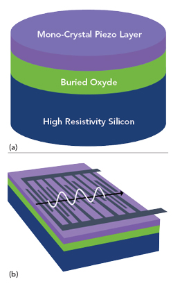
Figure 1 Structure of the POI engineered substrate (a) and resulting SAW propagation (b).
Because it is no longer possible to compromise on some of the performance criteria and in response to the more stringent requirements demanded by the new 5G network features, Soitec has developed a new engineered substrate that enables operators and phone makers to respond to these challenges. POI engineered substrates consist of a thin layer of single-crystal piezo material (today single-crystal lithium tantalate) on top of a SiO2 layer and a high resistivity silicon substrate as shown in Figure 1a. The top lithium tantalate thickness typically ranges from 0.3 to 1 μm. This thin film POI engineered substrate is built using Soitec Smart-Cut™ technology which allows for high uniformity layers and high-quality volume manufacturing.
This structure guides the acoustic wave at the surface of the substrate and confines its energy in the top thin lithium tantalate layer with very low losses (see Figure 1b). With this engineered substrate, filter designers have access to a substrate material with a better coupling factor (k2) and a lower thermal expansion coefficient. This enables them to design resonators with a high-quality factor at higher frequencies and target larger bandwidth filters with low temperature sensitivity. It also provides the capability to integrate multiple filters on the same die.
The POI substrate is composed of three layers, a piezoelectric material, a buried oxide and a silicon layer. The thin and highly uniform piezoelectric layer confines the energy of the guided wave, enabling high performance acoustic characteristics. The buried oxide selects and guides only high velocity waves and constrains the piezo material, reducing thermal expansion and in-turn temperature sensitivity. This structure allows for high signal selectivity, as well as frequency stability when temperature changes. Therefore, it also simplifies the manufacturing process compared to TC-SAW since filter device manufacturers do not need to add a thick layer on top to constrain the piezo material, thus improving the coupling efficiency.
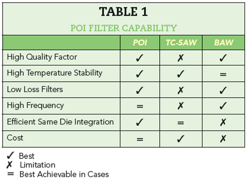
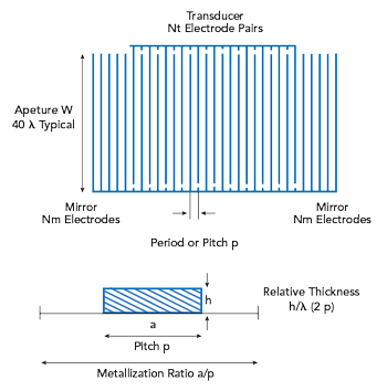
Figure 2 SAW resonator design.
The very low insertion losses achievable by a SAW filter designed on a POI substrate allows device manufacturers to efficiently manage energy consumption. Compared to existing solutions, SAW filters on POI have a high Q-factor, high coupling for large bandwidth filters, extremely low TCF and efficient integration of filters on the same die (see Table 1).