

An electrostatic discharge (ESD) is the sudden flow of current between two electrically charged objects, caused by the breakdown of the dielectrics separating them, i.e., dielectric breakdown. In the case of electronic devices, the resulting current flow and possible spark can permanently damage the device (see Figure 1). An often recited yet unsubstantiated quote is “...losses associated with ESD in the electronics industry are estimated at between half a billion and $5 billion annually.” In reality, estimating the exact cost of ESD loss is extremely difficult; nonetheless, ESD forces the development and testing of many hardware prototypes during design and manufacturing and contributes to a high number of warranty claims with loss of consumer confidence if a failure occurs in the hands of the consumer. Therefore, electronics manufacturers go to great lengths to properly shield sensitive components and design systems to reduce, dissipate and neutralize static charge.
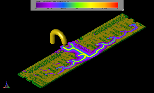
Figure 1 Electric fields during a simulated ESD test of a DDR3 RAM stick.
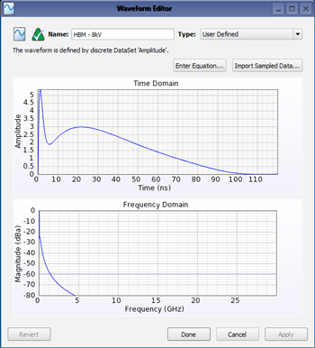
Figure 2 8 kV HBM waveform in XFdtd.
To test ESD susceptibility, hardware engineers typically use test models defined by various standards, from organizations such as ANSI, JEDEC and the IEC. The most common and widely used ESD models are the human body model (HBM), which approximates a discharge from a charged human fingertip to a grounded device (see Figure 2), and the charged device model (CDM), which approximates a discharge from a charged device to another conducting object at a lower electrostatic potential. These tests are generally performed using ESD simulators or ESD guns to apply high speed and high voltage pulses to various points of the device under test (DUT).
Even for an experienced engineer, pinpointing the location of an ESD failure during testing - or determining whether a failure occured at all - can be extremely challenging. ESD failures are typically categorized in three groups: catastrophic, latent or upset. In the case of a catastrophic failure, the DUT no longer functions and there is usually physical damage such as melted and/or charred components. Intuitively, a catastrophic failure may sound like the worst-case scenario; however, it is actually the most ideal to encounter during quality assurance testing, because it is easily recognized, located and accounted for in the final ESD mitigation design. On the other hand, latent and upset failures are much more difficult to diagnose because the DUT still functions, with little or no sign of physical damage. Latent failures are often not visible to the naked eye and result in a weakened device which functions at the time of testing and deteriorates over time with continued usage, often malfunctioning or failing in the consumer’s possession. Upset failures result from over-currents which do not physically damage the DUT but compromise the components’ semiconductive properties, leading to unpredictable behavior and data loss in use. Latent failures can sometimes be identified with magnification, but upset failures are nearly impossible to detect during testing.
Given the high cost of time and materials for ESD hardware testing and the difficulty locating latent and upset failures, simulating ESD testing is extremely valuable, as it can pinpoint locations susceptible to ESD damage and then help optimize ESD mitigation during product design. Responding to this growing need, new ESD simulation features have been added to Remcom’s full wave electromagnetic simulation software package, XFdtd®. Using XFdtd’s improved user-defined waveform feature, engineers can import ESD waveforms defined by various testing standards, using them to create ESD current sources in an XFdtd project. At this point, ESD simulator/gun models can be created and used to excite the DUT geometry at locations of interest, with the resulting electromagnetic (EM) fields and current flows simulated and analyzed (see Figure 1).
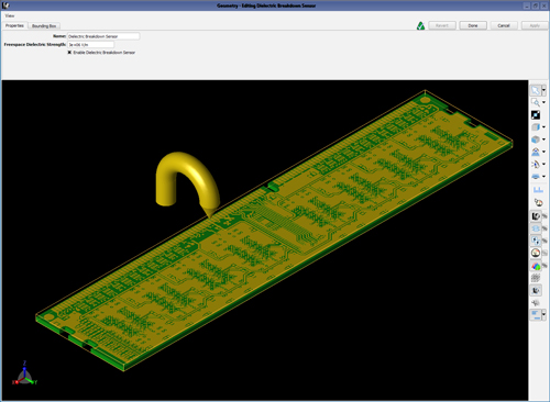
Figure 3 Definition of dielectric breakdown sensor.
To solve the challenge of determining if and where an actual ESD failure occured, a new material parameter, dielectric strength, was added to XFdtd’s electric material definitions. The dielectric strength of a material defines the maximum electric field it can withstand without experiencing dielectric breakdown (i.e., losing its insulating properties). Upon adding the dielectric strength parameter to XFdtd, it is possible to monitor FDTD cell edges for potential breakdown during transient simulations using a dielectric breakdown near-field sensor (see Figure 3). The sensor instructs the XFdtd calculation engine to monitor cell edges for electric fields exceeding the dielectric strength of their constituent materials, recording instances when dielectric breakdown is likely to occur. The sensor requires the user to define the free space dielectric strength, used for all edges that do not contain a defined material. The default free space dielectric strength is set to 3 MV/m, the dielectric strength of air at sea level. The sensor also allows the user to define a bounding box to limit the volume monitored for dielectric breakdown. Using this feature saves on computation by defining the specific areas of interest, rather than examining the entire computational domain. At the conclusion of an FDTD simulation, the cell edges which exceed their respective dielectric strengths can be viewed, as shown in Figure 4.

Figure 4 Risk areas for dielectric breakdown identified during simulated ESD testing.
Functionality was also added to XFdtd to monitor specific electronic components that are taxed beyond their rated voltage and current input parameters, which can be obtained from the components’ data sheets. Post-simulation results identify those components that are subject to permanent damage due to unsafe limits (see Figure 5).
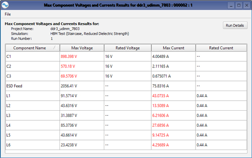
Figure 5 Summary of components exceeding rated design parameters during simulated ESD testing.
While simulation cannot and should not replace hardware testing entirely, these new computational features provide ESD engineers with more insight into the probable locations of ESD failure, enabling ESD mitigation designs to be optimized prior to prototyping hardware. Remcom believes this capability will reduce product development cost and time to market, while improving product reliability and consumer confidence. These new features lay the foundation for additional multiphysics capabilities, including plasma discharge and thermal simulation to model the current and heat generated from spark discharges. Merging these computational techniques will enable the analysis of downstream current flows after an initial dielectric breakdown, more accurately predicting dielectric and circuit component failures.
Remcom
State College, Pa.
www.remcom.com