

The RF market is developing faster than ever. Wireless communication is present everywhere - home, office, factory and vehicle, with new applications developing at high speed. Without wiring and bulky connectors, miniaturization and simplicity are easier to achieve with new designs. Making this possible and inexpensive, RF antennas and circuitry are often moved to the printed circuit board (PCB); hence, fast prototyping is essential to prove circuit layouts and quickly release these new products to the market. To help designers fabricate prototype boards quickly, the first tabletop LPKF laser etching system, ProtoLaser ST, offers excellent performance using popular high frequency substrates from Rogers and other manufacturers.
GEOMETRIC PRECISION
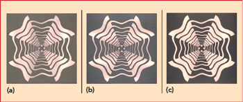
Figure 1 Logarithmic periodic antenna fabricated on RO3003 (a), RO4003 (b) and RT5880 (c) substrates with the ProtoLaser ST.
Using LPKF CircuitPro PL 3.3, with predefined laser tool parameters from the supplied materials library, LPKF evaluated the performance using a wideband antenna design as a test vehicle, comparing the geometry of the design with physically measured results on fabricated samples. The demonstration evaluated the copper wall quality, surface damage and processing time.
A planar logarithmic periodic wideband antenna, measuring 60 mm x 60 mm, was fabricated with the ProtoLaser ST, using LPKF’s “hatching” algorithm, where larger areas of conductive material are removed by slicing it into smaller pieces and then delaminating it from the board. After processing, the boards were cleaned with the LPKF cleaner and a soft brush. Figure 1 shows samples using Rogers RO3003, RO4003 and RT5880, with substrate thicknesses of 510, 410 and 254 µm, respectively, and a common Cu thickness of 18 µm on both sides. For a direct comparison, the same geometry was used for each board, despite the different RF properties of the substrates. The ProtoLaser ST’s ultra-flat ceramic vacuum table holds the thinnest and most sensitive materials in place, stress-free: in this case, the 10 mil thick and very soft RT5880.
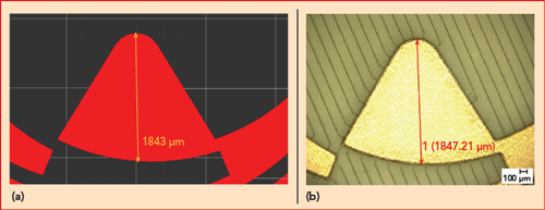
Figure 2 CAD design (a) vs. fabricated sample on RO4003 (b).
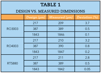
The primary concern with any fabrication technique is geometric precision. The logarithmic periodic antenna has a complicated geometry, a good test vehicle to demonstrate the capabilities of the laser etching process. The layout at the center of the antenna, at the electrical connection point, provides a good assessment of the laser’s ability to achieve the track and gap widths and curved features (see Figure 2). All measurements were performed at the same position, with the same approach and using a Keyence VHX-1000 digital microscope. The design values, measured data and calculated deviations are shown in Table 1. These largely minor dimensional differences can be improved by optimizing the parameters for the material and compensating the design dimensions after measuring the performance.
SURFACE, WALLS AND SPEED
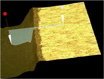
Figure 3 Profile of a laser-cut side wall on RO5880.
LPKF has patented a method for removing large areas of copper from the substrate: first cutting these areas into thinner tracks - called hatching - then using laser heat to delaminate the material. After cutting through the copper, depending on the substrate composition, minor scribe lines on the substrate surface may be seen using a microscope, as seen in Figure 2b. The laser cut is straight and smooth, yielding near-perfect walls. The walls may be inclined a few degrees outward (see Figure 3), a slight chamfer which is opposite to the under etching with wet technology.
The size of the sample used for this evaluation was 60 mm x 60 mm, 36 cm2, and the average processing time with the three Rogers samples was 212 seconds each, a processing speed of 10 cm2/minute. Processing a reasonably sized 100 cm2 board (10 cm x 10 cm) will take approximately 10 minutes - probably less time than required to solder a pair of RF connectors to a board to measure the performance.
FLEXIBILITY
A new granite base and perfectly flat vacuum table enable thin flexible materials and foils to be positioned freely and held precisely. The LPKF ProtoLaser ST is compact and economical, the first high-end tabletop laser etching system requiring only a single-phase power socket and compressed air to operate. As with all LPKF ProtoLaser systems, the ST has a large laser safety window for monitoring the process and laser class 1 qualification to ensure operator safety and convenience.
Design data from RF simulation software can be imported into LPKF CircuitPro with a few clicks via DXF or a vector format. Intuitive software guides the user, beginning with selecting the material and laser tool through the steps to fabricate a finished PCB. Libraries of proven materials and tools enable a quick start for prototyping, and users can add custom tools to the library for unique materials.
Offering fast processing and compatible with a wide range of materials, the LPKF ProtoLaser ST enables efficient prototyping of complex digital, analog and RF/microwave circuit boards. It supports single or double sided boards and multiple technologies on the same substrate. The laser system achieves exact geometries on almost any material, fabricating complex geometries such as antennas, filters and other applications where precise, steep sidewalls are required.
With additional equipment, the LPKF ProtoLaser ST can produce multilayer boards. The latest generation of the powerful CAM and machine software, LPKF CircuitPro, handles data preparation and system control in a single package. CircuitPro is optimally designed to process substrates prepared with an LPKF ProtoMat. Together with the integrated camera system, the software enables the exact positioning of pre-drilled and cut-out PCBs. CircuitPro guides users through the production steps for multilayer boards, simplifying the process for the user.
LPKF Laser & Electronics
AG Garbsen, Germany
www.lpkf.com