
TUTORIAL
Microwave Temperature Compensated Detector Design for Wide Dynamic Range Applications
Fundamentals on RF detection, Schottky diode matching techniques, temperature compensation schemes and video output system configurations are reviewed.
Modern radar and communications systems usually include and make use of intelligent management of their transmitter output power. The main goals achievable through this function go from interference elimination in systems sharing the same operating frequency range to configuration of low probability of interception (LPI) systems, where a spatial management of the output transmitted power may even constitute a system requirement. Also, the reliability of the transmitters must be ensured through the use of power sensors to implement built-in test equipment (BITE) functions. To this effect, transmitters should include power detectors capable of efficient and precise operation over wide power and temperature ranges.
This article presents the key design features necessary for this kind of detector. Fundamentals on RF detection, Schottky diode matching techniques, temperature compensation schemes and video output system configurations are reviewed. As an example, an X band detector design is presented, which makes use of a low cost commercial packaged Schottky diode (MA4E2054 by M/A-COM). It achieves an RF input power range greater than 35.0 dB and ±0.3 dB peak error due to temperature changes within the range 25° to 85° C. The detector's performance was tested and measured within a 10 percent bandwidth centered at 9 GHz.
For temperature compensation purposes, it will be demonstrated through simulation results that large signal operation of the nonlinear element is more suitable. However, large signal operation cannot be obtained for the desired wide range of RF input power levels, so small signal operation is also necessary if a dynamic range larger than 35 dB is desired. Small and large signal simulations were carried out making use of the Advanced Design System (ADS) by Agilent Technologies. Expressions to determine the optimum working point for small signal operation matching, temperature compensation effects and wide RF input dynamic range are also included.
RF DETECTION FUNDAMENTALS
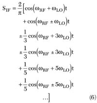
Microwave detector diodes use the nonlinearity of the junction resistance for their operation. If a sinusoidal RF input signal is assumed (ΔV = Vp cos(ωc t)), the current through the nonlinear element can be expressed using Taylor's expansion,1,2 as
The DC component in Equation 1 can be expressed as
where i(V0 ) is the bias current term, and the second term is due to the presence of the RF input signal and depends on the RF power level through Vp .
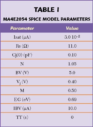
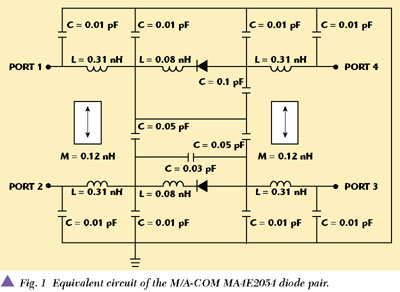
The characteristics of the diode to be used in the proposed example are given in Table 1. Figure 1 shows the packaged device equivalent circuit, which includes two Schottky diodes.
|
|
|
The basic expression that relates the voltage drop across the Schottky diode and the current through its terminals is given by

The most commonly used and simplest small signal equivalent model for a Schottky diode is presented in Figure 2. Three basic elements are required to model the behavior of this device under small signal operation:
|
|
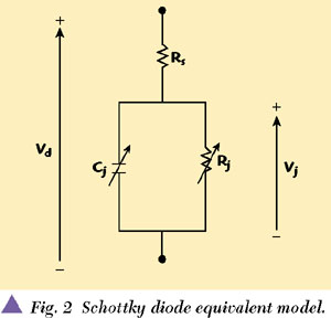
The junction resistance (Rj ) is the inverse of the I-V slope relationship and can be expressed as
where
|
Is |
= |
saturation current |
|
I0 |
= |
DC current through the diode |
The series resistance (RS ) represents ohmic contacts and substrate losses.
The junction capacitance (Cj ) depends on the voltage drop. Cj should be small enough so as not to shunt the RF current across the diode's resistance Rj . A parameter that allows the measurement of the device's efficiency is the cutoff frequency fc defined as

DETECTION SCHEMES
Single Diode Detection Configuration
The most common diode-based detection scheme found in the bibliography is shown in Figure 3,13 which also shows the key elements of a conventional RF detector:
|
|

 RF filtering and matching network/RF input power equalization: It is important to notice at this point that the input RF matching should be obtained not just for the whole working bandwidth, but also for the whole range of RF input power levels (for large signal operation).4 In the case considered here, since a large dynamic range (larger than 35 dB) was desired, this feature was used as a way to make even larger the dynamic range of the detector through the use of power equalization under large signal operation. The key idea is to prevent the diode from saturating at a rather low input signal power level. In order to do so, the designed detector takes advantage of the fact that the behavior of the input matching network will depend on the input signal power level.5 The detector is purposely unmatched at high input power levels of the RF signal, thus extending the input power dynamic range as desired.
Also, the use of lumped components has been avoided as much as possible for low cost and mounting considerations. The input matching network was entirely designed making use of distributed elements.
The RF choke is the return path for the DC rectified component and behaves as an open circuit for the RF signal.
The Schottky diode is the nonlinear element where harmonically related components (as well as DC current) are generated from the RF signal.
The output capacitor is necessary to avoid the presence of RF signals (the fundamental frequency and the generated harmonics) at the detector's video circuit through the use of a grounded capacitor.
The video circuit, in the case of the simple scheme presented, is a single resistance.
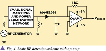
The basic RF detection scheme presents two main problems. The first one is the fact that the detector RF performance is influenced by the value of the video output resistor.5 The change of the output resistance in the basic scheme completely modifies the diode's biasing point for a specific RF input power level. It would be desirable to have both the RF input detection stage and video voltage processing block well isolated, so that both can be modified without disturbing each other's behavior. In order to do so, an operational amplifier (op-amp) was used, as shown in Figure 4. With this new scheme, the RF stage has at its output a shortcircuit at RF (due to the grounded output capacitor) and also a shortcircuit at the DC component (due to the operational amplifier virtual ground), thus making RF and video stage isolation complete.
|
|
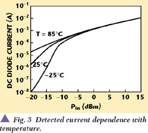
The second problem associated to the basic scheme is the strong dependence of the detected current on temperature, especially at low RF input levels. If a large power range is required over a wide working temperature range, then this dependence must be eliminated. Both detected current and input matching depend on the diode junction resistance (Rj ), which at the same time depends on temperature. In order to study more precisely this dependence it is necessary to make use of large signal simulation tools. Large signal operation was simulated with the LSSP6 circuit simulation block from ADS.
Figure 5 shows the simulated results obtained for the detected current in the scheme using an op-amp as a function of the RF input power level and temperature.
|
|
The dependence of junction resistance with temperature for small signal operation is
The temperature dependence of junction resistance is due to two factors: direct dependence with temperature and dependence through saturation current as
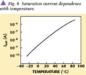
The temperature dependence of the saturation current of the specific diode used in this design is shown in Figure 6.
Diode Biasing
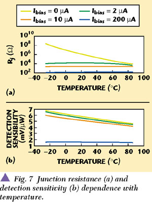
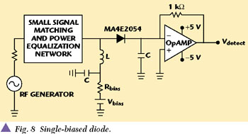
The solution given to the temperature dependence problem was the addition of bias current,1 which reduces both junction resistance and detection sensibility K(mA/µW) dependence with temperature (see Figure 7), and also facilitates the diode matching by reducing the junction resistance.
|
|
|
The biasing network, shown in Figure 8, is formed by three simple elements: the RF choke, biasing resistance (Rbias ) and biasing voltage (Vbias ).
|
|
The reduction of junction resistance dependence with temperature is easily demonstrated by the inclusion of the Ibias term in Equation 6.

In fact as (Ibias >> Isat ) Rj may be expressed as

Also including Ibias reduces the direct dependence of Rj with temperature as
However the addition of Ibias introduces an offset term in the current flowing through the diode (Idiode ), which may be expressed as
|
Idiode |
= |
Ibias (T) + Idet + Isat | |
|
|
* |
Ibias (T) + Idet | |
|
|
= |
Ibias (T) + K(T)Pin |
(11) |
where
Ibias (T) = biasing current which depends on temperature
K(T) = detection sensitivity (mA/µW) which depends on temperature
Pin = RF input power level
For temperature compensation it is necessary to eliminate Ibias (T).
Two Diode Configuration
The elimination of Ibias (T) is done by means of another diode biased at the same point as the first one.7 The current through this second diode is
Idiode2 = Ibias (T) (12)
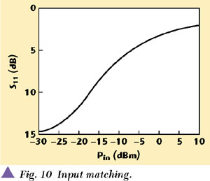
Temperature compensation of the offset term is obtained if the bias current through each diode is made equal. With all these points in mind the final detector configuration is shown in Figure 9. Figure 10 shows the diode input matching as a function of the RF input power level.
|
|
|
|

RESULTS
Four different configurations are presented next to show the design process previously explained.
Single Diode Detection Scheme
First, a single diode detector configuration (basic scheme with op-amp) was measured. The final configuration was mounted and measured, but it made use of just a single diode in order to evaluate the need of the second diode to compensate for the temperature dependence of the offset term.
The input matching network was designed following the ideas given in the preceding section for large signal power equalization and small signal matching. The biasing parameters were chosen keeping in mind that:
If Vbias is set too large then at low RF input power levels the detector will not have any resolution because the current through the diode will be mostly that of the biasing network.
Rbias should be selected so that Ibias allows simple matching at the detector's input for small signal operation.
These considerations led to the selection of Vbias = 0.32 V and Rbias = 820 Ω. The resulting measured response of the detected voltage versus RF input power is shown in Figure 11. In order to compare the improvements obtained at each step of the designing process, power detection errors were evaluated. The measured absolute error obtained in this configuration is also shown in the figure.
|
|
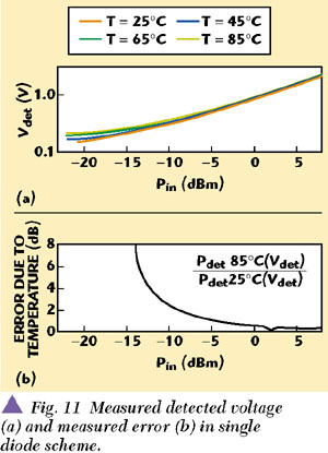
Two main conclusions can be drawn from these measurements:
Ibias reduces significantly the detected voltage dependence on temperature changes.
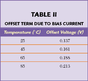
The detected voltage includes an important offset term due to bias current, as shown in Table 2, that should be removed in order to improve the RF input dynamic range.
|
|
Two Diode Detection Scheme (Same Bias)
Results obtained after including the temperature compensation diode are given in Figure 12. Both diodes were biased making use of the same biasing network previously described.
|
|
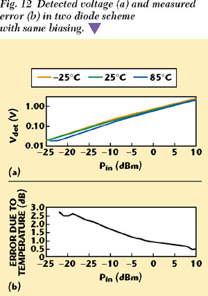
The offset term is eliminated through the use of this second diode7 and the detectable power range has increased. Nevertheless, because of the use of low cost components for the video processing stage (low cost operational amplifiers) the offset term is not totally canceled and detected power errors are still significant. Also, although errors due to temperature changes have significantly decreased, peak detection error at low input power levels is still too great for precision detection applications. This is due to the fact that the detection sensitivity K(T) varies with temperature (Equation 11).
It is possible to correct the K(T) effect previously explained and further obtain substantial improvements with respect to the detector's behavior by making some small modifications.
As previously stated, the current through each diode is given by
Idiode1 = Ibias1 (T) + K(T)Pin
Idiode2 = Ibias2 (T) (13)
The key idea is to bring together the responses of the detected voltage for different temperatures at low RF input signal power levels, where errors mainly occur. This could be done by slightly modifying the biasing parameters for the offset cancellation diode, as will be explained next.
For a given low input power level (Pinlow ), and for the range of working temperatures [Tmax , Tmin ], the detected current at the limits of the temperature range is given in each case by
Idet (Tmin ) = Ibias1 (Tmin )
+ K(Tmin )Pinlow Ibias2 (Tmin )
Idet (Tmax ) = Ibias1 (Tmax )
+ K(Tmax )Pinlow Ibias2 (Tmax ) (14)
It would be desirable to have
Idet (Tmin ) = Idet (Tmax ) (15)
so that no errors appear at Pinlow . The condition of Equation 15 may be accomplished by modifying Ibias of the diodes used in the design. If Equation 15 is met, then, as the rest of the detector's temperature responses are enclosed between those at Tmax and Tmin , the reduction of errors is evident.
Two Diode Detection Scheme (Different Bias)
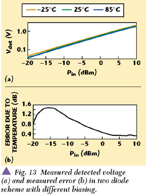
In order to meet the requirements of Equation 15 (for Pinlow = 22 dBm) the biasing parameters for the first diode were maintained (Vbias1 = 0.32 V and Rbias1 = 820 Ω), while those of the second diode where changed to Vbias2 = 0.32 V and Rbias2 = 910 Ω.
Results obtained after performing this change are given in Figure 13. The error due to temperature has been almost eliminated through the use of different bias parameters for each diode.
|
|
Final Detection Scheme
When different biasing is used for each diode the output current is given by
Idet (T) = K(T)Pin + Ibias1 (T) Ibias2 (T)
= K(T)Pin + ΔIbias (T) (16)
For low RF input signal power levels ΔIbias (T) compensates the K(T) variations due to temperature drifts. In the preceding case, for Pin = 15 dBm, the term K(T)Pin is much greater than ΔIbias (T) and thus compensation cannot occur.
If K(T) is made smaller through the use of a greater value of Rbias1 then ΔIbias (T) will be able to compensate for K(T) changes due to temperature for Pin values even larger than 15 dBm.
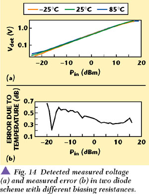
Rbias1 was chosen to be Rbias1 = 1.5 kΩ and Rbias2 was calculated to meet condition 15 (Rbias2 = 1.8 kΩ). Results obtained after performing this change are given in Figure 14.
|
|
CONCLUSION
In this work, basic design rules and key aspects for implementing power sensors operating under wide power and temperature ranges have been presented through different design examples. In each case experimental results and simulations have successfully confirmed the proposed step-by-step design technique.
ACKNOWLEDGMENTS
This work was supported by INDRA SISTEMAS and Project TIC-1999-1172-C02-01/02 of the National Board of Scientific and Technology Research (CIYCIT). The authors would like to acknowledge José Luís Jiménez-Martín for his valuable suggestions.
References
1. I. Bahl and P. Bhartia, Microwave Solid State Circuit Design, John Wiley & Sons, 1988.
2. D.M. Pozar, Microwave Engineering, John Wiley & Sons, 1998.
3. "Schottky Barrier Video Detectors," Application Note 923, Hewlett Packard, 1986.
4. "Impedance Matching Techniques for Mixers and Detectors," Application Note 963, Hewlett Packard, 1980.
5. Harrison and Polozec, "Non-square Law Behaviour of Diode Detectors Analyzed by the Ritz-Galerkin Method," IEEE Transactions on Microwave Theory and Techniques, Vol. 42, No. 5, May 1994.
6. "Diode Detector Simulation using Hewlett-Packard EESOF ADS Software," Application Note 1156, Hewlett Packard, 1998.
7. R.J. Turner, "Schottky Diode Pair Makes an RF Detector Stable," Electronics, May 1974, pp. 9495.
|
|
 Germán Torregrosa- Penalva received his Ingeniero de Telecomunicación degree from Universidad Politécnica de Madrid, Madrid, Spain, in 1999, and is currently working toward his PhD degree at the Dpto. de Señales, Sistemas y Radiocomunicaciones, E.T.S.I. Telecomunicación, Universidad Politécnica de Madrid. His research activities are in the area of high frequency circuit design and radar systems.
  Alberto Asensio-López received his Ingeniero de Telecomunicación degree from Universidad Politécnica de Madrid, Madrid, Spain, in 1984, and his PhD degree at the Dpto. de Señales, Sistemas y Radiocomunicaciones, E.T.S.I. Telecomunicación, Universidad Politécnica de Madrid in 1990, where he has been an associate professor since 1991. His research activities are in the area of high frequency circuit design and radar systems.
  Jaime Lluch-Ladrón de Guevara received his Ingeniero de Telecomunicación degree from Universidad Politécnica de Madrid, Madrid, Spain, in 2000, and is currently working at Telefonica Reseach and Development Department. His research activities are in the area of mobile communications solutions.
  F. Javier Ortega- González received his Ingeniero de Telecomunicación degree from Universidad Politécnica de Madrid, Madrid, Spain, and his PhD degree at the Dpto. de Señales, Sistemas y Radiocomunicaciones, E.T.S.I. Telecomunicación, Universidad Politécnica de Madrid. His research activities are in the area of high frequency circuit design, electromagnetism and radar systems.