
Diamond has been sought out by many researchers and companies for heat spreader application for years due to its excellent thermal conductivity (1500 W/mK). It has been shown that utilizing a diamond heat spreader can enhance RF performance by 20 percent compared to standard GaN on SiC devices.
In 2014, Element Six acquired Group 4 with the goal of improving GaN on Diamond (GoDi) epitaxial wafers, mainly the quality and thermal characteristics of the chemical vapor deposition (CVD) diamond layer. Significant improvements in the CVD diamond deposition process lead many researchers to successfully triple the power density of GaN transistors utilizing diamond as the substrate.1
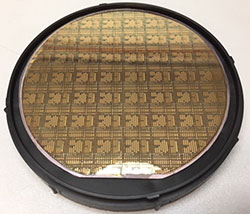
Figure 1 4-in. GaN on Diamond finished wafer.
With ongoing demands for higher power density, smaller form factor and better RF performance throughout the market, RFHIC acquired, in a 2016 partnership with Akash Systems, intellectual property related to GoDi technology from Element Six. Figure 1 shows a photo of a 4-in. GoDi epitaxial wafer. The process involves taking a GaN on Si wafer and removing the silicon substrate completely so that CVD diamond layer can be directly deposited on to the GaN surface.
Various successful demonstrations of GoDi HEMT devices show excellent thermal and RF performance has been developed in the past but most work utilized small wafers (less than 4-in.) for fabrication. With the help of RFHIC’s foundry partner, fully automated 4-in. fabrication of GoDi HEMT process is now possible. For GaN HEMT process flow, standard GaN on SiC process flow is used for production with minimal process modifications. Because GoDi HEMT wafers are very thin (about 120 μm thick), special carrier bonding techniques which could withstand various processes had to be developed.B
Because diamond is the hardest natural element, scribing and via holes cannot be done with standard blades or etch processes. This led RFHIC to investigate laser as the source for both scribing and via hole drilling. RFHIC has managed to successfully make via holes and scribing with streets narrower than 60 μm wide with lasers. RFHIC is also looking into a newly developed plasma etching process that could significantly increase via hole process.
Currently, qualification 4-in. wafers are in the final steps of processing and measurements will be available in June 2018. A follow-up article is planned to detail the results of these development efforts.
References
- F. Ejeckam, D. Francis, F. Faili, D.J. Twitchen, B. Bolliger, J. Felbinger and D. Babic, “S2-T1: GaN on Diamond: A Brief History,” Lester Eastman Conference on High Performance Devices, August 5-7 2014, DOI: 10.1109/LEC.2014.6951556. INSPEC Accession Number: 14775316.
- M. Wu, D. Hou and W.S. Lee, “Fabrication of 4-in. GaN/Diamond HEMT in a Compound Semiconductor Foundry,” CS Mantech 2018, Austin, Texas.