
LTE uplink carrier aggregation (ULCA) puts new, significant linearity challenges on RF front-end components. The switches need to be ultra-linear to achieve the best receive sensitivity, with an input third-order intercept point (IIP3) greater than 90 dBm required to achieve uncompromised performance.
RF Innovation has developed a technology—SwIP®—that improves third-order intermodulation (IM3) performance of FET-based switches by greater than 20 dB (see Figure 1), which boosts switch linearity to levels of 95 dBm IIP3. While this technology can be used in many applications where ultra-linear switches are required, LTE ULCA is probably the most prominent since the benefits are dramatic. Many concepts have been developed that try to overcome the shortcomings of limited IM3 performance in RF front-ends, but all of them require extra effort and cost, such as separate antennas for the two uplink carriers. Now, SwIP technology allows an easier, smaller and more cost-effective solution for RF front-ends.
LTE ULCA CHALLENGES
LTE carrier aggregation (CA) has almost unlimited possibilities to combine available spectrum. The uplink case puts tough linearity requirements on the RF front-end components, requiring unprecedented IIP3 levels. While LTE without uplink CA requires approximately 72 dBm IP3, adding uplink CA increases this to greater than 90 dBm, because mixing products can fall into the receive bands and reduce receive sensitivity (see Figure 2). For example, for uplink inter-band CA of bands 1 and 3, the intermodulation products of the two transmit (Tx) carriers fall into the band 1 receive (Rx) and GPS spectrum, respectively. A similar issue occurs for uplink CA of bands 2 and 4, where the upper IM3 product falls into the band 2 Rx spectrum. 3GPP specifications acknowledge the technical challenge and allow maximum sensitivity degradation (MSD) up to 25 dB.
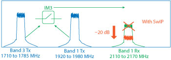
Figure 1 SwIP reduces IM3 products, boosting LTE carrier aggregation performance.
SwIP TECHNOLOGY
Most of this loss of sensitivity can be regained using SwIP technology. SwIP has been developed by RF Innovation to help meet these requirements and uses existing semiconductor processes. The main features and benefits of SwIP are:
- Up to 20 dB improvement in IMD3, boosting IP3 to 95 dBm
- Process agnostic: applicable for bulk CMOS, SOI and GaAs PHEMT
- Power agnostic: applicable for any power level
- No impact on isolation
- Approximately 0.1 mm² die area
- Approximately 0.05 dB added insertion loss.
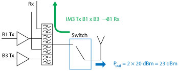
Figure 2 With uplink carrier aggregation, antenna switch creates unwanted IM3 products that fall into band receive frequencies.
Figure 3 shows the performance improvement SwIP technology adds to a standard SPDT switch implemented in SOI. A SOI-based SPDT has an inherent IP3 of 83 dBm, the performance that commercially-available, high IP3 switches offer today. Using SwIP, IM3 products are 20 to 25 dB lower, increasing IP3 by 12 dB to an absolute level of 95 dBm.
The price paid for this IM3 improvement is a minor insertion loss increase of approximately 0.05 dB and approximately 0.1 mm2 additional die area compared to the baseline SPDT. The isolation is identical to that of the baseline SPDT. A sensitivity analysis simulating production, voltage, temperature and load VSWR swings shows robust behavior.
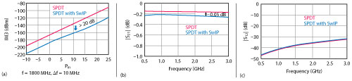
Figure 3 SPDT IM3 (a), insertion loss (b) and isolation (c) using SwIP technology.
The benefits of SwIP technology were verified with demonstration hardware fabbed on a 180 nm SOI process. Compared to a SPDT switch without SwIP, the first tape-out hardware achieved:
- IMD3 improvement of 15 to 20 dB
- Approximately 0.1 dB additional insertion loss
- Identical isolation.
APPLICATIONS
LTE ULCA is one of the targeted applications for SwIP technology, as it enables highly linear RF front-ends with IIP3 up to 95 dBm. However, its usage is not limited to mobile phone switches; it covers any RF switch application requiring extraordinary high linearity with power levels up to tens of Watts. SPDT, DPDT and more complex configurations with multiple inputs and outputs can be supported.
The technology has been proven with SOI hardware and has been successfully evaluated for GaAs PHEMT and bulk CMOS processes.
RF Innovation is offering SwIP intellectual property rights to interested parties for licensing or acquisition.
RF Innovation
Starnberg, Germany
www.rfinnovation.de