
Duplexer Considerations for X-band T/R Modules
A transmit/receive (T/R) module’s duplexer plays a critical role in determining a phased array’s reliability, radar cross section (RCS) and performance. Several different block diagrams are typically used to realize the duplexer, but many common configurations do not satisfy basic duplexer requirements. This article discusses the capabilities of the three most common duplexer configurations as well as supporting component design considerations.
Renee Z. Jones and Bruce A. Kopp
The Johns Hopkins University, Applied Physics Laboratory
Laurel, MD
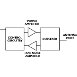
A duplexer connects a phased array’s transmitter and receiver to an individual radiating element, as shown in Figure 1 . Since the duplexer insertion loss will directly degrade antenna noise figure and radiated power, it should provide a low loss connection from the antenna element to either the transmitter or the receiver. A duplexer also must have directional properties to ensure efficient phased-array operation (that is, transmitter energy is directed to the radiator, not the receiver, and received signals go into the receiver, not the transmitter).
 In addition to these requirements, the duplexer must isolate the transmitter and receiver from reflected or external signals. The level of isolation required can be determined from the phased array’s intended operating environment and the receiver and transmitter design. Reflected energy into the duplexer can be created by many circumstances including a broken connector, ice on the radome or objects with a high RCS near the antenna.
The minimum level of duplexer protection is typically set equal to the transmitter’s output power. The future use of wide bandgap power amplifiers will significantly increase the level of protection required. The amount of energy that is re-reflected by the duplexer is also important to control the phased-array RCS.
The final significant issue is load pulling. The antenna element’s impedance varies as a function of scan angle and is often as high as 3:1 at large scan angles. This large variation can cause a corresponding variation in the output power as a function of scan angle. A duplexer must isolate the transmitting amplifier from impedance variations of the antenna element to prevent significant load pulling.
Circulator/Balanced Limiter Duplexer
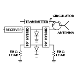 A circulator and balanced diode-limiter, shown in Figure 2 , can be used to satisfy all of the aforementioned T/R module duplexer requirements. The circulator directs any energy into the antenna to the receiver and any transmitter energy out of the antenna with less than 0.5 dB insertion loss at X-band.1 The circulator will also typically isolate the transmitter from the input energy by > 15 dB. Very high receiver protection can be provided by limiter diodes. Reflected signals are dissipated in the input coupler 50 W load, and will prevent transmitter load pulling. This circuit will provide good RCS performance during receiver, transmitter or unbiased operation.
An isolator can be used instead of the balanced limiter to terminate the reflected limiter energy. However, this configuration typically is not used since an isolator often costs more than the additional limiter diodes and 90º couplers. The balanced circuit also doubles the limiter’s power handling capability. If the receiver’s low noise amplifier is placed within the balanced circuit its third-order intercept point also can be increased by 3 dB.
A circulator/balanced limiter may not provide adequate transmitter protection if the input 90º hybrid does not provide a good impedance match at the frequency of interest. This condition typically occurs outside of the coupler’s normal operating bandwidth, and the signals are generally reduced by antenna and circulator impedance mismatches before they reach the 90º hybrid. A lowpass filter also can be inserted between the antenna element and the duplexer to provide increased isolation from external systems above the antenna’s operating bandwidth.
Circulator/Limiter/Switch Duplexer
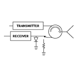 A single-pole double-throw (SPDT) switch, limiter and circulator are also often used as a duplexer, as shown in Figure 3 . The switch is connected to the 50 W load during transmitter operation. The circulator and 50 W load protect the receiver and transmitter during transmission. This configuration also prevents load pulling of the transmitter and provides good RCS performance.
The switch is connected to the limiter during receive operation. The limiter then protects the receiver, but reflected limiter energy will be directed to the transmitter by the circulator. Transmitter isolation is provided solely by resistive losses along the microwave path. Excessive energy input from other systems can then lead to transmitter damage. This circuit also has poor RCS performance during the reception of signals large enough to turn the limiter on, unless a balanced power amplifier is used.
Limiter/Switch Duplexer
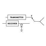 An SPDT switch and limiter also may be used for the duplexer function, as shown in Figure 4 . This circuit is often attractive as a low cost option that allows the duplexer to be integrated with a transceiver MMIC. The switch provides no protection to the transmitter from reflected transmitted energy or external inputs. The transmitter is also not isolated from the antenna and load pulling can occur during scanning.
If a balanced power amplifier is used in the transmitter, RCS issues can be minimized during transmission. The balanced power amplifier still can be damaged by excessive inputs into the antenna during transmission. Energy reflected during receive will degrade RCS.
This duplexer should not be used if the anticipated operating environment includes external systems capable of damaging the transmitter during transmission, if reflected transmissions can damage the transmitter or if a balanced power amplifier is not used to prevent high RCS at sufficiently wide scan angles.
Duplexer Component Design Considerations
Ferrite circulators are capable of providing robust performance for typical GaAs X-band applications and can support wide bandgap output power levels. The circulator cost is also typically less than five percent of the overall X-band T/R module cost. Active circulators have been proposed to provide lower cost,2 but possess noise figure and power handling limitations for typical X-band applications.
Silicon PIN diodes provide satisfactory performance for current T/R modules and will be able to address future wide bandgap applications. Active bias to lower the diode resistance can be used to provide improved thermal management and decreased leakage. Thermal management also often requires the limiter diodes to be placed on thermal spreaders or the use of a high thermal conductivity substrate. The resulting silicon hybrid limiter has few parts and relatively low assembly complexity. Hybrid limiters typically compose less than five percent of the total X-band module cost. The limiter also can be realized with GaAs active devices to reduce the assembly complexity associated with the silicon hybrid.3-5 However, the thermal conductivity of GaAs (0.47 W/cmºC) is considerably less than that of silicon (1.38 W/cmºC), and is a significant thermal design disadvantage.
 Thermal design considerations are also important for the input 90º coupler. This resistor terminates limiter reflections that add in-phase through the coupler. Excessive heat caused by power dissipation can destroy the resistor or permanently change its resistance value. If either condition occurs, the mismatched load will begin reflecting power back into the coupler. Reduced film temperatures may be achieved by increasing the resistor area and/or using a higher thermal conductivity substrate.
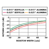
Resistor thermal management is offset by the desire to keep the resistor area small to provide good return loss at X-band. Increasing the resistor dimensions would decrease the film temperature but would also degrade the electrical performance, as shown in Figure 5 . Thus, a BeO substrate, or material with similar thermal resistance, should be used in this case.
References
1. Trak C9A9A10 data sheet (www.trak.com).
2. S. Hara et al., “Novel Unilateral Circuits for MMIC Circulators,” IEEE MTT Proceedings , October 1990, pp. 1399-1405.
3. D.G. Smith et al., “Designing High-power Limiter Circuits with GaAs PIN Diodes,” IEEE MTT-S, 1999.
4. C. Trantanella et al., “An Investigation of GaAs MMIC High Power Limiters for Circuit Protection,” IEEE MTT-S, 1997.
5. GaAsTEK ITT313503D data sheet (www.gaastek.com).
6. J.E. Sergent and C.A. Harper, Hybrid Microelectronics Handbook , McGraw-Hill Inc., 1995.
Renee Z. Jones received her BSEE and MSEE from Virginia Tech and Johns Hopkins University, respectively. Currently, she is a senior staff member at The Johns Hopkins University Applied Physics Laboratory (JHU/APL) and works in the Radar Systems Development Group. Since joining JHU/APL in 1993, Jones has analyzed phased-array radar system performance and currently specializes in microwave and RF subsystems.
Bruce Kopp received his BSEE from Arizona State University and his MSEE from Stanford University. Currently, he is employed at the Johns Hopkins University Applied Physics Laboratory developing solid-state microwave technology, T/R modules and associated phased-array antenna hardware. Kopp also teaches a short course on T/R modules. Previously, he worked at Avantek as a microwave and RF component and system design engineer.