
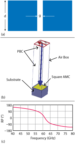
Figure 1 Square AMC’s two unit cells (a) HFSS setup (b) and reflection phase (c).
This article presents a 60 GHz circular patch Antenna-on-Chip (AoC) on asymmetric Artificial Magnetic Conductor (AMC) designed and fabricated using the TSMC 0.18 µm CMOS process. An AMC plane allows a positive reflection coefficient within the bandwidth of interest so incident and reflected waves are in phase. At the AMC frequency of operation, a high impedance is generated which reduces surface waves and thus enhances gain. At first, circular AoC performance is enhanced using a square AMC. However, square AMC cells suffer from discontinuities that affect performance when using lengthy feed lines to connect the AoC to a front-end circuit. To overcome this problem, an asymmetric rectangular (R-AMC) is employed. A modified asymmetric AMC is used with a circular AoC for further gain enhancement. The area of the fabricated design is only 1715 µm x 710 µm. Measured |S11|, gain and radiation patterns are reported.
The 60 GHz Band has an unlicensed bandwidth of 7 GHz (from 57 to 64 GHz), which allows for a high data rate of several gigabytes/sec, surpassing the capability of current wireless technologies. The exploitation of this frequency band is of interest for a variety of emerging applications such as uncompressed high definition video streaming, mobile distributed computing, wireless gaming, internet access, fast large file transfer and wireless personal area networks. The 60 GHz Band has several advantages such as the possibility for frequency reuse over small distances due to high oxygen attenuation of 10 to 15 dB/km, and the prospect for antenna miniaturization as the free space wavelength is 5 mm at 60 GHz. These advantages enable a 60 GHz system to be a suitable replacement for current short range wireless systems.1-3
System-on-Chip (SoC) is a promising solution for low cost wireless communication since it integrates the antenna, front and back-end circuits on one chip. Integration of the AoC with other circuits eliminates the costs associated with materials required for external antennas. Moreover, antenna matching circuits are eliminated as a 50 Ω boundary is no longer required. Finally, SoC enables a one step foundry fabrication of the entire wireless system. For further cost reduction, the cost effective CMOS process, a digital mainstream technology, is used to implement the AoC. Since the CMOS substrate is characterized by low resistivity and high permittivity; however, AoC performance is poor in terms of gain and radiation efficiency.1-16
Post processing design methodologies such as micro-machining4 and proton implantation5 are used to improve AoC performance. Micromachining improves performance by selectively removing parts of the lossy CMOS substrate underneath the AoC.4 Proton implantation enhances performance by implanting high energy ions in the area below the AoC, increasing CMOS substrate resistivity.5 Even so, these two techniques increase the overall cost due to the additional processing. Electromagnetic shielding using Artificial Magnetic Conductor (AMC)3,11-14 is another alternative. An AMC plane is composed of periodic metal patches in two or three dimensional configurations over a dielectric substrate. The AMC plane is characterized by a reflection coefficient of +1 at its center frequency, which enables wideband matching. In the AMC operating frequency band, high impedance is acquired due to the planar dimensions, leading to reduced surface wave propagation; hence, radiation efficiency of the AoC is enhanced. However, an AoC employing a symmetric AMC11-14 suffers from a low gain to active area ratio. To enhance its gain to active area ratio, Barakat et al.,3 introduced a method to increase the number of AMC cells in the direction of AoC polarization and limit the number of AMC cells in the perpendicular direction.
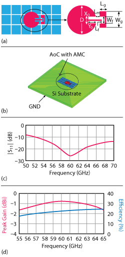
Figure 2 Circular AoC with AMC plane; top view (a) 3D view (b) simulated |S11| (c) and simulated peak gain and efficiency (d).
In this article, the use of an asymmetric rectangular (R-AMC)15 is proposed in order to increase the gain to active area ratio without affecting other performance characteristics. Furthermore, an asymmetric R-AMC has a reduced insertion loss for extended feed lines when compared to a symmetric AMC. The design is optimized using the ANSYS High Frequency Structure Simulator (HFSS®) and the layout is done using Cadence Virtuoso®. Implementation is in 0.18 µm CMOS technology.
CIRCULAR AoC WITH SQUARE AMC
The reflection phase on an AMC plane varies with the frequency between ±180° and equals zero at its resonance frequency. The useful bandwidth of the AMC is generally defined in the range between ±90°.3 The percentage AMC bandwidth (BWAMC) can be expressed by
where fup and flo are the frequencies at which the reflection phase equals +90° and -90°, respectively. While, fc is the center frequency at which reflection phase equals 0°.
A square AMC unit cell3 is shown in Figure 1a and the simulation setup to optimize its reflection phase response is shown in Figure 1b. Periodic boundary conditions (PBC) are realized using Perfect-E and -H boundaries. A wave port is used as an excitation port. The reflection coefficient (S11) is embedded at the surface of the AMC unit cell and the reflection phase response is computed as the angle of the embedded S11. The optimized dimensions of the square AMC are d = 260 µm and g = 30 µm with a bandwidth of 16.5 percent.
The square AMC is then used to enhance the performance of circular AoC following the approach described by Cohn.16 According to this methodology, the gain to active area ratio of the AoC is enhanced by increasing the number of AMC cells in the direction of antenna polarization and decreasing them normal to this direction. The circular AoC with optimized AMC plane is shown in Figures 2a and 2b and its optimized dimensions are listed in Table 1. The simulated |S11| is shown in Figure 2c showing a bandwidth of 18 GHz. Its simulated gain and efficiency are -0.8 dBi and 22.5 percent, respectively, at 60 GHz as shown in Figure 2d.
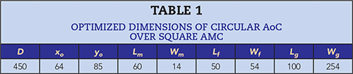
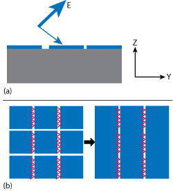
Figure 3 AMC in presence of incident TM wave; incident wave with E-field in yz-plane (a) original AMC and equivalent asymmetric AMC (b).
CIRCULAR AoC WITH ASYMMETRIC R-AMC
For a TM case, a wave with its E-field in the yz-plane and H-field in the x-direction as shown in Figure 3a is incident on a “Cohn square” in free space.16 The observed E-field in the plane of the square AMC vanishes in the space between the edges parallel to the y-direction, thus reducing the square AMC to a strip array of asymmetric R-AMC as shown in Figure 3b.17
The asymmetric R-AMC is used to enhance the circular AoC as shown in Figure 4a and its dimensions are found in the same way as for a square AMC. The simulated |S11| of the circular AoC with asymmetric R-AMC and with square AMC are compared in Figure 4b, showing no change in the resonant frequency and approximately the same matching performance. Gain and efficiency of the circular AoC with asymmetric R-AMC and with square AMC are compared in Figure 4c. Approximately the same behavior is observed in both cases. Similarly, the electric field distribution in both cases is almost identical as can be interpreted from Figure 4d. These observations show that square AMC and asymmetric R-AMC are equivalent for TM mode antennas.
CIRCULAR AoC WITH MODIFIED ASYMMETRIC R-AMC
In order to further enhance the AoC gain to active area ratio, the asymmetric R-AMC plane is modified as shown in Figure 5 by removing the two cells directly below the AoC. AMC cell removal for increased gain was initially proposed by X. Bao et al.11Additionally, the unit cell is limited in length (L) from 860 µm to 710 µm since in this direction the gain performance is negligibly affected. After that, the input matching of the AoC is improved by adding circular rounds to the AMC cells near to the AoC as shown in Figure 5a and then by optimizing the gap between the AoC and the modified AMC cells “d1” and the separation between the modified cells “d2”. The simulated |S11| and peak gain responses of the antenna are shown in Figure 5b. This antenna has a gain of 0 dBi at 60 GHz and its area is only 1.19 mm2.
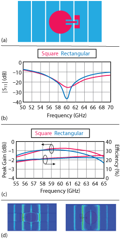
Figure 4 Circular AoC with asymmetric AMC plane; top view (a) simulated |S11| (b) simulated peak gain and radiation efficiency (c) current density with square AMC (left) and asymmetric R-AMC (right) (d).
LAYOUT, FABRICATION AND MEASUREMENTS
The layout of the circular AoC with modified asymmetric R-AMC plane is shown in Figure 6a with a slight change in the feed position. The area is 1715 µm x 710 µm. The fabricated AoC chip photo is shown in Figure 6b with the measurement setup shown in Figure 6c. The antenna is characterized using the measurement set-up described by Pan et al.,19 using a 100 µm Infinity® probe. The calibration is done using a Cascade 101-190 calibration kit. The AoC is placed using supporting foam which is nearly invisible to the EM waves. A piece of metal is placed below the chip to account for the package ground. Measured and simulated |S11| of the fabricated AoC are compared in Figure 6d. The measured results show good agreement with simulation.
Simulated and measured peak gain responses of the fabricated AoC are compared in Figure 7a. Since the actual fabricated AoC is located on a chip corner, its simulated gain, noted as “no metals,” is compared with measured results. Initially, a discrepancy of up to 4 dB is found between the measured and simulated results. Since simulated surrounding environment is metal free,18 the discrepancy may be due to nearby metals, probe pins and the probe body which are not considered in simulations. In the simulation model shown in Figure 7b, nearby metals expected to affect the measurements are considered. The probe’s pins are modeled as suggested by Pan et al.19 The simulated peak gain noted as “with metals” in Figure 7a is in better agreement with the measured results especially for frequencies up to 58 GHz. Further discrepancies between measured and simulated gain may be due to other metals which are not modeled, and also due to the ± 0.8 dB accuracy of the measurement setup.18
Measured radiation patterns are shown in Figure 8. The E-plane and H-plane are located at XZ and XY cut planes, respectively as can be interpreted from the coordinate system in Figure 7b. The patterns show some twist especially for the E-Plane.
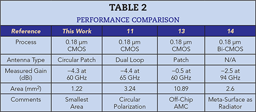
A performance comparison is shown in Table 2. Peak gain is the same or slightly lower than for other designs, while the fabricated antenna has the lowest chip area.
CONCLUSION
Asymmetric R-AMC is proposed for the purpose of enhancing gain and reducing the size of a circular AoC. The antenna design shows a peak simulated gain of -0.4 dBi at 60 GHz. The actual AoC, fabricated using 0.18 µm CMOS technology, demonstrates a peak measured gain of -4.3 dBi at 60 GHz with an overall area of 1.22 mm2. Initial discrepancies in simulated versus measured gain are resolved by re-simulating the fabricated AoC considering probe pins and nearby metals expected to affect performance. Agreement between simulation and measurement is found for frequencies lower than 58 GHz. For higher frequencies, discrepancies on the order of 1.5 dB may be due to other nearby structures not considered in simulations. Measured and simulated radiation patterns are in good agreement.
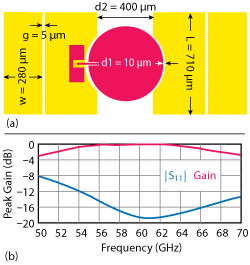
Figure 5 Circular AoC over asymmetric R-AMC; top view (a) simulated |S11| and peak gain (b).
References
- P. Smulders, “Exploring the 60 GHz Band for Local Wireless Multimedia Access: Prospects and Future Directions,” IEEE Communications Magazine, Vol. 40, No. 1, January 2002, pp.140–147.
- F. Gutierrez, S. Agarwal, K. Parrish and T. S. Rappaport, “On-Chip Integrated Antenna Structures in CMOS for 60 GHz WPAN Systems,” IEEE Journal on Selected Areas in Communications, Vol. 27, No. 8, October 2009, pp.1367–1378.
- A. Barakat, A. Allam, R. K. Pokharel, H. Elsadek, M. El-Sayed and K. Yoshida, “Compact Size High Gain AoC Using Rectangular AMC in CMOS for 60 GHz Millimeter Wave Applications,” IEEE International Microwave Symposium Digest, June 2013, pp. 1–3.
- R. Wang, Y. Sun, M. Kaynak, S. Beer, J. Borngräber and J. C. Scheytt, “A Micromachined Double-Dipole Antenna for 122 – 140 GHz Applications Based on a SiGe BiCMOS Technology,” IEEE International Microwave Symposium Digest, June 2012, pp. 1–3.
- K. T. Chan, A. Chin, Y. P. Chen, Y. D. Lin, T. S. Duh and W. J. Lin, “Integrated Antennas on Si, Proton-Implanted Si and Si-on-Quartz,” International Electron Devices Meeting Technical Digest, December 2001, pp. 40.6.1–40.6.4.
- H. M. Cheema and A. Shamim, “The Last Barrier: On-Chip Antennas,” IEEE Microwave Magazine, Vol. 14, No. 1, January 2013, pp. 79–91.
- A. Shamim, L. Roy, N. Fong and N. G. Tarr, “24 GHz On-Chip Antennas and Balun on Bulk Si for Air Transmission,” IEEE Transactions on Antennas and Propagation, Vol. 56, No. 2, February 2008, pp. 303–311.
- Y. P. Zhang, M. Sun and L. H. Guo, “On-Chip Antennas for 60-GHz Radios in Silicon Technology,” IEEE Transactions on Electron Devices, Vol. 52, No. 7, July 2005, pp. 1664–1668.
- S. S. Hsu, K. C. Wei, C. Y. Hsu and H. R. Chuang, “A 60-GHz Millimeter-Wave CPW-Fed Yagi Antenna Fabricated by Using 0.18-μm CMOS Technology,” IEEE Electron Device Letters, Vol. 20, No. 6, June 2008, pp. 625–627.
- P. H. Park and S. S. Wong, “An On-Chip Dipole Antenna for Millimeter-Wave Transmitters,” IEEE Radio Frequency Integrated Circuits Symposium, June 2008, pp. 629–632.
- X. Y. Bao, Y. X. Guo and Y. Z. Xiong, “60-GHz AMC-Based Circularly Polarized On-Chip Antenna Using Standard 0.18-μm CMOS Technology,” IEEE Transactions on Antennas and Propagation, Vol. 60, No. 5, May 2012, pp. 2234–2241.
- L. Jiang, J. F. Mao and K. W. Leung, “A CMOS UWB On-Chip Antenna with a MIM Capacitor Loading AMC,” IEEE Transactions on Electron Devices, Vol. 59, No. 6, June 2012, pp. 1757–1764.
- H. H. Yeh, N. Hiramatsu and K. L. Melde, “The Design of Broadband 60 GHz AMC Antenna in Multi-Chip RF Data Transmission,” IEEE Transactions on Antennas and Propagation, Vol. 61, No. 4, April 2013, pp. 1623–1630.
- S. Pan, F. Caster, P. Heydari and F. Capolino, “A 94 GHz Extremely Thin Metasurface-Based BiCMOS On-Chip Antenna,” IEEE Transactions on Antennas and Propagation, Vol. 62, No. 9, September 2014, pp. 4439–4451.
- A. Barakat, A. Allam, H. Elsadek, H. Kanaya and R. K. Pokharel, “Small Size 60 GHz CMOS Antenna-on-Chip: Gain and Efficiency Enhancement Using Asymmetric Artificial Magnetic Conductor,” European Microwave Conference, October 2014, pp. 104–107.
- S. Cohn, “Electrolytic Tank Measurements for Microwave Metallic Delay-Lens Media,” Journal of Applied Physics, Vol. 21, No. 7, July 1950, pp. 674–680.
- S. Clavijo, R. R. Diaz, W. E. McKinzie, “Design Methodology for Sievenpiper High-Impedance Surfaces: An Artificial Magnetic Conductor for Positive Gain Electrically Small Antennas,” IEEE Transactions on Antennas and Propagation, Vol. 51, No. 10, October 2003, pp. 2678–2690.
- D. Titz, F. Ferrero and C. Luxey, “Development of a Millimeter-Wave Measurement Setup and Dedicated Techniques to Characterize the Matching and Radiation Performance of Probe-Fed Antennas,” IEEE Antennas and Propagation Magazine, Vol. 54, No. 4, August 2012, pp. 188–203.
- S. Pan, L. Gilreath, P. Heydari and F. Capolino, “Investigation of a Wideband BiCMOS Fully On-Chip W-Band Bowtie Slot Antenna,” IEEE Antennas and Wireless Propagation Letters, Vol.12, June 2013, pp. 706–709.
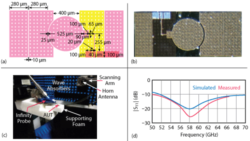
Figure 6 Circular AoC over modified asymmetric R-AMC; layout (a) photo of fabricated chip (b) measurement setup (c) and simulated vs. measured |S11| (d).
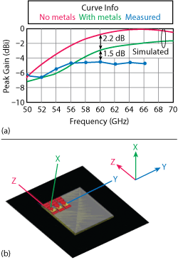
Figure 7 Measured gain vs. simulation (a) and HFSS model (b).
Adel Barakat graduated from Faculty of Engineering, Mansoura University, Egypt in 2008. He received his MSc. and Ph.D. degrees from Egypt-Japan University of Science and Technology (E-JUST), Alexandria, Egypt in 2012 and 2015, respectively and a part of his Ph.D. was a channel between E-JUST, Egypt and Kyushu University, Fukuoka, Japan in 2013-2014. His research interests include metamaterials, microstrip antennas, artificial dielectric layers, on-Chip antennas and on-Chip filters.
Ahmed Allam received his B.Sc. in electronics and communications engineering from Alexandria University, Egypt, followed by M.Eng. and Ph.D. degrees from the University of Alberta, Canada. Dr. Allam is currently an assistant professor in the department of electronics and communications engineering, Egypt-Japan University of Science and Technology. His research interests include the design of RF circuits and systems.
Hala Elsadek is a professor at Microstrip Department, Electronics Research Institute. She acted as department head from 2008-2012. Dr. Elsadek graduated from Faculty of Engineering, Ain Shams University, Cairo, Egypt 1991. Dr. Elsadek earned her master’s degree from University of Gunma, Japan in 1996 while her Ph.D. was through a channel between Cairo University, Egypt and University of California, Irvine, in 2002. Her research interests include wireless communications, electromagnetic engineering and microstrip antenna systems.
Adel B. Abdel-Rahman received his B.Sc. and M.Sc. degrees in electrical engineering, communication, and electronics from Assuit University, Assuit, Egypt, in 1991 and 1998, respectively, and the Doktor-Ing. degree in communication engineering from Magdeburg University, Magdeburg, Germany in 2005. He is currently with the department of electrical engineering, South Valley University, Qena, Egypt. His research interests include the design and analysis of antennas, filters, metamaterials, and its application in wireless communication as well as optimization techniques with applications to microwave passive devices and antenna arrays.
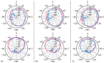
Figure 8 E-plane (top) and H-plane (bottom) radiation patterns; 56 GHz (a) 60 GHz (b) and 64 GHz (c). Measured (blue), simulated (red).
Ramesh K. Pokharel received his M.E. and Ph.D. degrees from the University of Tokyo, Japan in 2000 and 2003, respectively all in electrical engineering. He had been a post-doctoral research fellow with the department of electrical engineering and electronics at Aoyama Gakuin University, Japan from April 2003 to March 2005. In April 2005, he joined the department of electronics graduate school of information science and electrical engineering at Kyushu University where he is now a professor. His current research interests include the low cost RFIC and analog circuits for microwave and millimeter wave wireless communications, on-chip signal integrity issues and on-chip metamaterials in CMOS.
Aimeric Bisognin received his engineering degree in electronics from Polytech’Nice Sophia (Sophia Antipolis, France) in 2012 and his Master Propagation, Télédetection and Télécommunication from EDSTIC (Sophia Antipolis, France) in 2012. He is currently working towards his Ph.D. at the EpOC (Electronique pour Objets Communicants) laboratory from the University Nice Sophia-Antipolis and STMicroelectronics (Crolles, France). He is studying millimeter-wave communications, especially in the field of the design and measurement of antenna in package, lens and reflector antennas for 60, 80 and 120 GHz frequency bands.
Cyril Luxey received his DEA (master’s degree 1996) and Ph.D. in electrical engineering (1999), both with honors, from the University Nice-Sophia Antipolis, France. He has been a full professor at the IUT Réseaux et Télécoms in Sophia-Antipolis since 2009. He is doing his research in the EpOC laboratory where he is also the vice-deputy. His current research interests include the design and measurement of millimeter-wave antennas, antennas-in-package, plastic lenses and organuc modules for 60, 120 and 240 GHz frequency bands. Also, he collaborates with Berkeley Wireless Research Center and Stanford on mmWave front-end transceivers at mmWave frequencies; he also works on electrically small antennas, multi-antenna systems for diversity and MIMO techniques.