
For many microwave and millimeter wave applications, RF waveguides are the guided transmission technology of choice. Typically, waveguide interconnects and devices provide lower insertion loss and better VSWR than coaxial or microstrip transmission lines. Also, the high power handling capability, solid construction and high heat handling make waveguides particularly attractive to aerospace, military and scientific applications that require high power and performance. There are many nuances and easily forgotten factors to ensure waveguide assemblies and interconnects operate at maximum performance. It takes a good deal of knowledge to enter the waveguide game and, as many technologies rely on waveguides — especially millimeter wave — a lot of time and money can be saved with expertise.
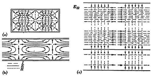
Figure 1 E22 mode field distribution in a rectangular waveguide: cross-sectional (a) longitudinal (b) and surface (c) views.1
TYPES, MODES AND FREQUENCY BEHAVIOR
The conductive walls of a closed circular, elliptical or rectangular waveguides facilitate the propagation of guided mode electromagnetic (EM) waves. There are several different modes for each type of waveguide (see Figure 1), and the equations that determine the frequency behavior of the modes are different for each type. For rectangular waveguides, the TE10 mode is the most commonly used, as it has the lowest attenuation. Rectangular waveguides also tend to be the most common type for components and assemblies. However, for routing purposes, circular or elliptical waveguide interconnects are commonly used for long runs. Waveguides are capable of multi-mode operation, but this may not be ideal since the interaction between the modes can degrade signal integrity for any single mode — when evanescent wave coupling occurs with higher modes, for example.
The lower frequency limit of a waveguide is a hard cutoff where the attenuation exponentially increases as the frequency lowers, disabling transmission (see Table 1). Most rectangular waveguides are specified with a 2:1 width to height ratio to achieve a maximum bandwidth ratio of 2:1, i.e., the ratio between the maximum frequency and minimum cutoff frequency. This way, maximum power is carried by the waveguide before microwave breakdown, dielectric breakdown or multipaction can occur. This differs from a circular waveguide since it can only propagate a maximum bandwidth ratio of 1.3601:1, which is the maximum single mode frequency to minimum cutoff frequency. The recommended frequencies of operation for a rectangular waveguide are 30 percent higher than the cutoff frequency and 5 percent below the cutoff frequency of the next higher mode. These recommendations prevent dispersion at the lower frequencies and multi-mode operation at higher frequencies.
Even if a waveguide is operated within the recommended frequency range, the group delay and phase delay over its entire bandwidth is a significant percentage of the speed of light (see Figure 2). This is unlike TEM mode transmission lines, such as coaxial transmission lines, which have a relatively flat group delay over their operational frequencies. Nonlinear phase or wide variations in group delay can cause fidelity errors in wide bandwidth radar systems and even intersymbol interference in wide bandwidth digital communication systems. Devices such as phase shifters are used to correct the phase delay from the waveguide response, component delays and unequal length routing.
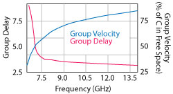
Figure 2 WR90 group delay and group velocity vs. frequency.
With a short length of waveguide interconnect, it may be difficult to measure the insertion loss, phase delay or VSWR. The extremely low insertion loss and other performance factors over a short length may be below the measurement capabilities of all but the highest performance vector network analyzers (VNA). The insertion loss may only be a small fraction of a dB, and the dynamic range of the VNA may not be adequate to differentiate the insertion loss from noise.
Though waveguides are generally very high performing, routing with coaxial cables is occasionally preferable, such as when several mating/demating transitions occur, the routing is very tight and complex or to reduce cost. For systems with a low noise amplifier (LNA), a waveguide segment may be used to route RF energy from the antenna to the LNA input, with the output of the LNA connected to a coaxial segment, as the biggest impact to the signal-to-noise ratio (SNR) and dynamic range (DNR) is loss before the input of the LNA. High power systems may also use waveguides to route high power signals at the input and output. Systems can convert from waveguide to coaxial, to take advantage of the lower cost coaxial routing, where higher insertion loss and poorer VSWR have less impact.
EM PHENOMENON, SKIN EFFECT AND MICROWAVE BREAKDOWN
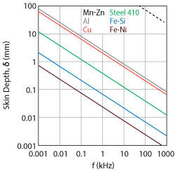
Figure 3 Materials with greater skin depth have less loss at high frequencies.2
At certain frequencies and power levels, the electrical and material properties of conductors and dielectrics can change and produce unexpected effects. At higher microwave frequencies, the electrons in a conductor migrate toward the surface, a phenomenon known as skin effect (see Figure 3). Also, if power levels are too high, the dielectric material between two conductors ionizes and becomes conductive, resulting in microwave dielectric breakdown. With skin effect, as the frequency of the EM energy in a waveguide increases, more of the traveling electrons migrate toward the surface of the inside walls of the waveguide. The inside walls are more significant to wave propagation than the outside surface of the waveguide, since the conductor’s high frequency conductivity is less in the bulk of the material than near the surface — a significant reason why high frequency losses in a conductor are much higher than low frequency losses.
For non-ferromagnetic conductors, the DC resistance is many times higher than at RF and microwave frequencies. Still, for ferromagnetic materials such as nickel, iron and steel, the AC resistance has a more significant increase with the greater magnetic permeability. For these reasons, very high conductivity metallization, such as silver and gold, are often used to plate the inside walls of a waveguide, especially for higher microwave and millimeter wave and power applications. At only 1 GHz, 98 percent of the electrons in a copper sheet are traveling within several micrometers of the copper sheet surface. At high microwave and millimeter wave frequencies, the region in which the majority of electrons travel is much smaller, making the surface conditions of the conductor extremely important. This means that the final plating material on the inside walls of a waveguide is often the only conductive material that has an impact on the EM propagation. Hence, surface conformity and smoothness are critical to reduce RF losses throughout the waveguide.
Another phenomenon that impacts high frequency and high power systems is the EM energy induced dielectric breakdown between the conductive walls of a waveguide that can cause high energy arcing. The arcing that occurs within a waveguide at high power can cause standing waves at extreme power levels and induce potentially damaging heat or even deplating the surface metals of the waveguide material. The power threshold where microwave breakdown occurs depends upon the dielectric properties, temperature, distance between conductors, frequency and pressure of the gaseous dielectric inside the waveguide. For high power waveguide filters, the spacing of the filter cavities with the surrounding metal is also important to prevent multipaction3 (see Figure 4). Gases with higher breakdown properties can be injected into a waveguide system to increase the power threshold before microwave breakdown occurs. After assembly, waveguide systems are sometimes purged of humid air with dry gases to prevent condensation and humidity that will reduce the microwave breakdown threshold. Specially made flanges with gas inlet and outlet valves are used for this.
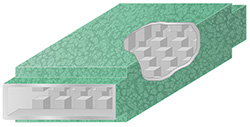
Figure 4 In complex waveguide components, calculating the necessary spacing at various power levels requires predicting material properties.4
QUALITY COUNTS
The quality of construction and materials can have a large impact on the performance of a waveguide system, especially at microwave frequencies and when carrying high power. Such waveguide can become difficult to manufacture and evaluate, as the tolerances are extremely small at microwave and millimeter wave frequencies. To achieve the necessary millimeter wave component and interconnect quality, soldering must be performed with a detailed visual inspection to ensure that no pits or holes exist in the solder. In space applications, even minute holes or pits can allow flux to leak from the material, increasing losses and degrading performance (see Figure 5). Machining tolerances for waveguides can be very tight, not only to ensure mechanical stability and strength but also because RF performance depends upon the precise relationship between the geometries, the plating and the smoothness of the inside waveguide walls and flanges. Any tooling marks or imperfections in the material can cause losses, reduced VSWR as well as misalignment when connecting with other waveguide components.
Though there are many reputable and high quality waveguide suppliers, some — particularly offshore — may streamline machining techniques to reduce manufacturing time and cost. These shortcuts can dramatically degrade waveguide component and system performance. Any misalignments or machined geometries beyond specified levels can increase the VSWR and allow RF leakage between the flanges, leading to increased maintenance and service costs. One example is the drilling of fastening holes in a waveguide flange. To achieve high precision alignment, the waveguide flange needs to be attached to the waveguide prior to drilling. However, some machining houses will drill the waveguide flanges prior to attachment. This results in xy and rotational displacement between the waveguide flange holes and the specified locations for the waveguide size and flange type. The errors may be so slight that they aren’t visually discernable or measurable with a pair of calipers. However, highly precise xy-coordinate machines are available to measure hole dimensions and can be used to evaluate incoming parts. Some high microwave and millimeter wave waveguides use guide pins, with detailed specifications provided in MIL-DTL-3922 (see Figure 6). At higher frequencies, these pins are specified to be 0615; however, some companies will use 0612 pins, as they are a standard stock pin. Although the differences in pin sizes are not discernible to the eye, the wrong guide pin can lead to misalignments.
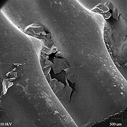
Figure 5 Minor contamination on plating can induce failures. Poorly plated silver led to the failure of a waveguide transfer switch array in NASA’s Mars Reconnaissance Orbiter (MRO).5
MECHANICAL AND MACHINING CONSIDERATIONS
Waveguides are predominantly constructed entirely with conductive metals, with the exception of pressure windows, some gaskets and jacketing materials. Generally, this means that waveguides are constructed in machining facilities by technicians knowledgeable in waveguide construction. Some of this knowledge is based on physics, such as the proper bend radius and lengths of bends; some depends upon experience gained through trial, error and troubleshooting. For instance, generic flexible waveguides tend to have poorer RF performance, i.e., insertion loss and VSWR, even though they may solve routing, misalignment and vibration challenges. Nonetheless, if a flexible waveguide is made with the appropriate sized sections for a specific frequency, the insertion loss and VSWR can nearly match a solid waveguide over a very narrow bandwidth. Additionally, some suppliers will perform a fully assembled flexible waveguide to reduce the occurrence of mechanical stress on a flexible waveguide segment that often causes the decoupling of the flex segments.
For waveguide twists and bends, there are very simple physics-based rules to follow to ensure that RF performance is optimized (see Figure 7). With rectangular waveguide, bends can be in the width for distorting the electric field, known as an E-bend, or the bend can be in the height wall for distorting the magnetic field, known as an H-bend. The radius required to have an optimal performing bend is greater than two wavelengths at the lowest frequency of interest. For a 45 degree twist, or sharp bend, the simple rule is that the outer wall length should be one quarter of the wavelength of interest. With sharp bends, the phase of the output signal will be inverted compared to the input, and the bandwidth will be limited compared to other routing options. With twists, a 90 degree bend requires at least two wavelengths, where a 180 degree twist requires four wavelengths for a full inversion. The polarization of the RF energy is changed during a twist and may need to be corrected, depending upon the system.
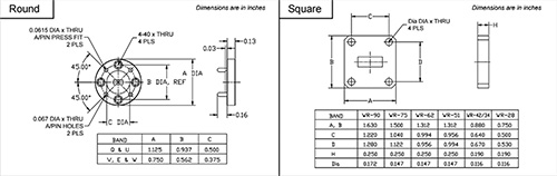
Figure 6 MIL-DTL-3922 defines the dimensions of waveguide flanges.6
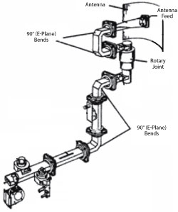
Figure 7 A properly designed waveguide bend will not cause additional loss or reflection, critical in long waveguide runs.7
Another area of concern for many waveguide purchasers is cost, due to the amount of gold plating on many waveguide products. For higher frequency microwave and millimeter wave applications, precious metal plating is necessary to minimize losses in the waveguide but is only needed on the inside surface of the waveguide and flanges. The plating on the outside surface of the waveguide, or plating on waveguides used at lower frequencies, is purely cosmetic or used to reduce corrosion. In this case, a much lower cost passivation layer may suffice.
ASSEMBLING: TROUBLESHOOTING AND HANDLING
Though waveguide components and interconnects tend to be formed of relatively sturdy metals, some aluminum and copper waveguides for higher frequency and aerospace applications can easily be dinged and dented. While these dings and dents are sometimes a useful tuning technique, they can dramatically change the performance of a waveguide or waveguide component. Ensuring proper packaging and shipping can prevent untimely surprises upon arrival. As shock and vibration during shipping can misalign the fittings, some suppliers will ship a waveguide assembly attached to a keeper plate to mitigate shipping and storing issues.
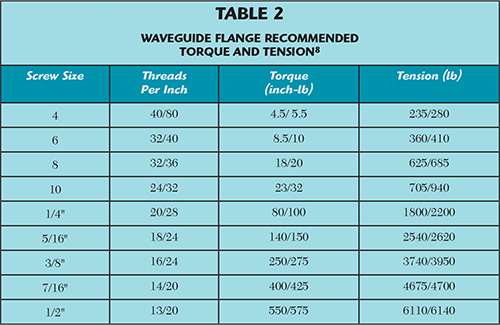
After receiving, the assembly and care of the waveguide component and interconnect can impact performance. One frequent issue is the attachment of the waveguide flanges. If no gasket is used, the surface of each flange needs to be clean and flat. Any marring, dust or peeling plating can lead to RF leakage and reduced performance from misalignment. Waveguide bends and twists may also form stress cracks from thermal cycling and mechanical stress. The higher the frequency of the waveguide, the more sensitive the system performance is to proper assembly and care. With flange attachments, a consistent and specified amount of torque should be applied at each corner (see Table 2). If one corner of a waveguide is torqued more or less than the others, a small gap will form and degrade VSWR and insertion loss. RF leakage can occur. This can also happen as a gasket degrades with age or heating/cooling cycles. Threaded screws can back up under vibration and heavy loading. Methods that ensure stable fastening should be used, as long as they do not impact RF performance and even clamping of the flanges.
If higher than expected loss or VSWR occurs, the next step is to track down the area of leakage. Rather than pulling the system apart and testing each connection, a detector probe can be used to scan an assembly for leakage points while running a test. Keeping a reasonable distance by using probes that prevent human contact with the waveguide assembly is recommended to avoid arcing, as RF leaks can lead to high voltage occurrences.
Conclusion
The low insertion loss, incredible VSWR and high frequency and power handling capabilities of waveguides comes at a price: a large learning curve and careful design and assembly. Some of the physics-based knowledge of waveguides can be found in a good book. However, there is a large amount of practical knowledge about construction and system design that is rarely available outside an experienced waveguide manufacturer and system design team.
References
- N. Marcovitz, “The Waveguide Handbook,” Isha Books, 2013.
- Zureks, “Skin Depth by Zureks,” Wikimedia Commons, 2011, Retrieved from commons.wikimedia.org/w/index.php?curid=13826795.
- H. M. Wachowski, “Breakdown in Waveguides Due to the Multipactor Effect,” Aerospace Corp., 1964, Retrieved from www.dtic.mil/dtic/tr/fulltext/u2/601069.pdf.
- Spinningspark, “Waffle-iron filter,” Wikipedia, 2011, Retrieved from en.wikipedia.org/w/index.php?curid=33584290.
- Jet Propulson Laboratory, “Contamination from Flaked Silver Plating Off Waveguides and Microwave Components,” 2008, Retrieved from llis.nasa.gov/lesson/1878.
-
Ducommun Technologies, 9. Technical Reference, Undated, Retrieved from www.ducommun.com/pdf/technicalReference.pdf.
Author unknown, “Radar Antenna Feed Waveguide,” NEETS Navy Electricity and Electronics Training Series, 1984, Wikimedia Commons, Retrieved from commons.wikimedia.org/w/index.php?curid=37229829. - Cobham Defense Electronic Systems, Waveguide Component Specifications and Design Handbook, Edition #7. Retrieved from www.cobham.com/media/102942/cmt-waveguide-handbook-part-2.pdf.