
Modelithics and Qorvo are collaborating to provide designers with free access to state-of-the-art high accuracy models for a growing number of power GaN transistors. The available and developing GaN model library supports simulation-based design flows for GaN power amplifiers (PA) with output power requirements from 5 W to over 500 W. This article summarizes the library content, features and devices as well as circuit level “closed loop” PA validations of the new models.
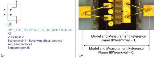
Figure 1 Die model schematic (a) and die with reference planes (b).
Microwave power amplifier design has been a hot research and development topic for several years now. What keeps the topic interesting and advancing is the interesting mix of new applications with challenging requirements, combined with ever changing technologies that have gone from Silicon to GaAs to GaN (and for a few applications back to Silicon) over the years. GaN has emerged as the clear technology winner for high power/high frequency applications and there are significant investments and rapidly evolving product advances in the worldwide GaN device and GaN power amplifier market.
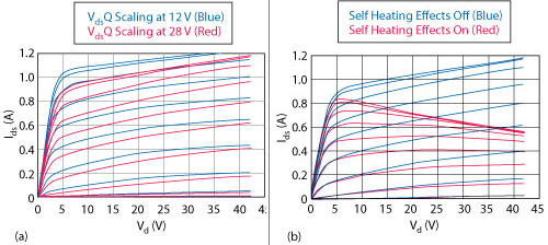
Figure 2 Quiescent bias voltage (VdsQ) scaling (a) and self heating effects (b) for the model of Fig. 1. Vgs range is -4 V to +1 V with a 0.5 V step.
Traditionally, microwave power amplifier design has been accomplished with a lot of know-how and very little if any computer simulation. For many the simple, but extremely practical “Cripp’s Technique”1 of load-line based analysis suffices to produce a simple starting point design that is built then taken to the lab where skilled technicians and engineers use their know-how to tune and tweak at the board level until desired specs are met.
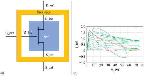
Figure 3 Intrinsic waveform sensing concept (a) and simulated dynamic load-line results for a packaged transistor at the extrinsic (blue) and intrinsic (red) nodes (b).
Others rely strictly on load-pull data to define their design criteria for achieving power amplifier output matching goals that achieve some desired compromise between output power, efficiency and linearity. A limitation is that load-pull data is expensive to acquire at each frequency and may not always be available at desired frequencies for new designs. Usually, bench tuning is still needed to achieve the desired performance goals.
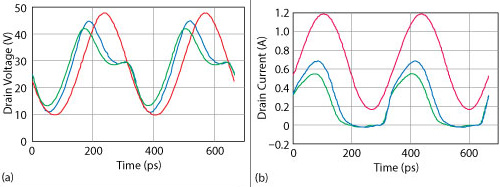
Figure 4 Intrinsic voltage (a) and current (b) waveforms for a TGF2023-2-01 transistor die at intrinsic reference planes for class A (red), class AB (blue) and class B (green) biasing, at backed-off power.
The classroom of “old school” PA design is clearly the power test bench, producing “graduates” who are experts in knowing how to move capacitors and foil around on a breadboard circuit to achieve desired goals. A very worthwhile skill indeed, and many PA gurus out there really know how to make these approaches work to produce excellent power amplifier products; however, this build-test-tune approach is not always the most efficient.
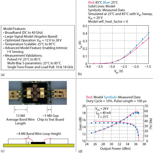
Figure 5 Model data sheet information for the large-signal version of the TGF2935 die model: features block (a) I-V model vs. measurement (b) fixture assembly (c) 10 GHz single tone power sweep, power matched (d).
The availability of accurate nonlinear models,2,3 combined with powerful EDA tools such as Keysight Technologies’ Advanced Design System and similar tools, has changed the paradigm of power amplifier design so that less time is spent on bench tuning. Instead, more and more PA designers start with model-enabled nonlinear simulation design flows, which increasingly can lead to design goals being met on the “first-pass” of fabrication and test, with little or no tuning. The availability of complete model-enabled PA circuit simulations allows for optimization of nonlinear circuit performance for complex sets of PA goals over either narrow or wide bandwidths. Nonlinear models provide significant benefits to designers who want quick turnaround designs, but may not have measured load-pull data at target frequencies. Such simulation capability can also be very useful in guiding post-fabrication adjustments, if needed, to improve or fine tune bench performance. As a result, many modern designers will not even consider using a new PA transistor if a model is not available. Another trend for many designers that want to use “waveform engineering”4 for optimizing high efficiency PA operating modes such as class B, AB, class F, and class J, among others, is the demand for access to intrinsic voltage and current ports.
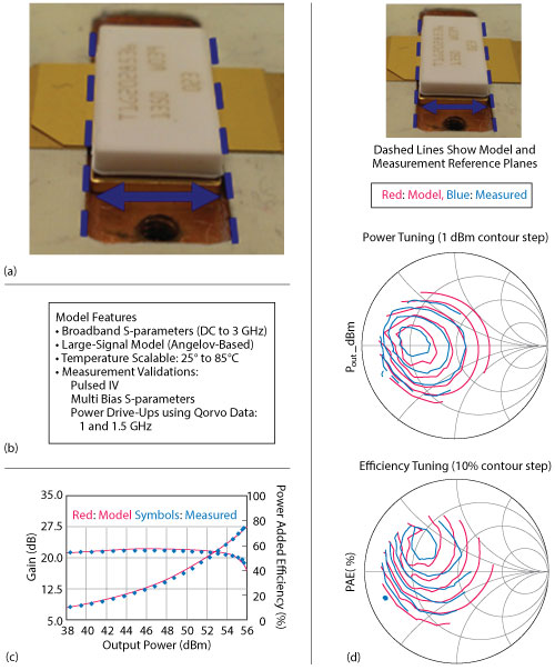
Figure 6 Load-pull and power drive up validations for Qorvo’s T1G2028536-FL-001 device (a) model features block (b) power swept validation at 1 GHz with power-tuned load (c), load-pull at 1 GHz on a 5 Ω Smith Chart and +35 dBm input power (d).
The Modelithics®-Qorvo GaN Library was created to meet the increasing demand in accurate nonlinear models for GaN devices by PA designers. This article describes the content, advantages and novel features of this growing library, and presents examples of validations being done to validate the quality and accuracy of the models at the device and circuit level. The library is currently available for use in Keysight Advanced Design System (ADS) and NI-AWR Design Environment. The library, model features and validations will be demostrated using Keysight ADS EDA software.
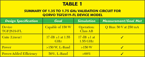
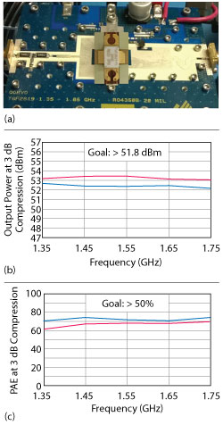
Figure 7 Assembled TGF2819-FL PA (a) with simulated vs. measured output power (b) and power-added efficiency (c). Red = simulation; blue = measurement average for five device samples mounted on one evaluation board.
GaN LIBRARY DESCRIPTION
The current version (1.7) of the library includes models for 17 die and 35 packaged devices, with many more models in development. The model library is set up to maximize designer convenience with a simple “click through” installation process and detailed model information data sheets accessible within the simulator. For example, in Keysight ADS, this is done simply by clicking the “Help” button on the model parameter pop-up window. The GaN Library is being distributed and supported by Modelithics for free, with sponsorship provided by Qorvo. Among the advantages of this arrangement is professionally managed software support, version control and frequent updates. With each update, additional models and model updates are provided and all models are kept up to date and operational with the latest EDA software revisions.
The GaN models themselves are currently based on a customized version of the Chalmers Angelov model.5 Advanced custom features of the models that benefit the designers include the following:
- Scaling of operating voltage (VdsQ)
- Ambient temperature and partial or full ON/OFF self-heating affects
- Intrinsic voltage/current node access for waveform optimization
- Switch to turn on/off bond wires for die models, as applicable.
Figure 1 shows a typical die model ADS symbol showing the user inputs for the model. VdsQ for this particular model can be scaled from 12 to 28 V, while other models in this library can have values as high as 50 V depending on the device nominal operating bias condition. This can be thought of as a “scalable” sweet spot for the model. This is in contrast to typical nonlinear models; although they are inherently bias scalable, they are generally tuned for best performance around a particular operating voltage. This bias scalability feature improves accuracy for variable bias conditions and, for example, takes into account the fact that the Pulsed I-V data used to build the model is different when pulsed from different VdsQ values as shown in the model results of Figure 2a.
The models allow the designer to take ambient and self-heating effects into account as well. Figure 2b shows simulation of I-V data with the “self heat factor” of Figure 1 set to 0 (no self-heating) and 1 (full self-heating, used for static bias/CW conditions). As another advanced custom feature, intermediate values between 0 and 1 can be used to estimate approximate partial self-heating effects of pulsed signals by setting the self heat factor equal to the duty cycle. Ambient temperature variation is provided by the “temperature” input to the model, which for this particular model is fit to temperature varied data over a range of 25° to 85°C. This range may vary as documented in the model information data sheet provided for each model.
The bond wire removal feature is provided for die models developed using fixtures with bond wires present. It allows users to conveniently either recreate the same simulation validations shown in the model information data sheet provided with bond-wires included, or remove the bondwires for embedding the model within their own unique circuit environments. This feature is not present in packaged devices, for models of die that can be directly wafer probed and for die models developed as scaled versions of measurement-based models from smaller die sizes.
Based on designer feedback, all models in the library provide for access to intrinsic voltage and current nodes for use in waveform analysis and optimization. Figure 3 illustrates the concept. The goal is to provide designers access to the voltage/current nodes at the model’s drain-to-source current generator plane while removing all parasitic effects. As seen in Figure 3b, the reactance of the parasitics causes the simulated dynamic load line to swing outside the constraints of the I-V plane, even to negative currents; properly extracted intrinsic waveforms do not. Figure 4 shows simulated intrinsic voltage and current waveforms. It is reassuring to see that the class A, B and AB currents are behaving as classically we would expect, with a full-wave current for Class A, half-wave rectified for Class B, and a similar, but reduced “conduction angle”6 waveform for the Class AB current.
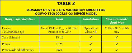
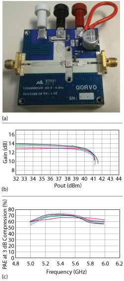
Figure 8 10 W, 5 to 6 GHz PA reference design (a) with simulated vs. measured output power at 5.4 GHz (b) and power-added efficiency vs. frequency (c). Solid lines = simulation, dashed lines = measurement of five PAs.
DEVICE LEVEL VALIDATIONS
The model information data sheet mentioned earlier is the key to understanding the details of each model contained within the library. These details include a model features block, detailed device level validations, and in some cases PA circuit level validations employing a reference design. Typical data sheets contain 15 to 20 pages (or more) of information. Example device validations include simulated model agreement to applicable measurements of current-voltage (I-V) characteristics, multi-bias S-parameters, load-pull data and Pout/PAE/Gt power swept data. Some device models also include fitting against noise parameter data.
Figure 5 contains a few snapshots of the type of information contained in the data sheets for one of the most recently added GaN die devices based on a 0.15 um technology process. As summarized in the model features block (see Figure 5a), this particular model for the Qorvo TGF2935 device was validated to 40 GHz for S-parameters and at 10 and 18 GHz for high power performance on a large-signal load-pull bench. A snapshot of simulated and measured I-V performance is shown at two temperatures (see Figure 5b). An assembly diagram clarifies reference planes and bond-wire details (see Figure 5c). A plot of swept transducer gain (Gt) and efficiency versus output power validates the model’s high power behavior against measured data (see Figure 5d). Large-signal and small- signal models are also available for the 0.15 um technology die devices that accurately predict noise parameters up to 26 GHz.
Similar information is provided for packaged device models as suggested by Figure 6, which includes selected information from the model data sheet for the 285 W Qorvo T1G2028536-FL-001 device. The model features block (see Figure 6a) shows that this model is validated to 3 GHz for S-parameters, is temperature scalable and is validated against high power data at 1 and 1.5 GHz. Also shown are plots of simulation versus measurement for load-pull and power drive up data.
PA CIRCUIT VALIDATIONS
In addition to the device level model validations discussed above, validations are also performed at the power amplifier circuit level. This section, discusses four examples of simulation-based PA reference designs that have been used for additional model validations of packaged device models from the GaN library. These PA designs range from medium to high power using several unique device models in this library, with each model displaying its value in achieving successful first-time designs. All of the designs presented are as measured after first assembly with no board tuning or bias adjustment.
For ‘closing-the-loop’ on initial measurements and simulations for these types of amplifier examples, detailed attention to the modeling of the passive matching and bias circuits is often found to be as important as the nonlinear model in terms of predicting the frequency dependent behavior of these amplifiers. Some board-dependent discrepancies are also significant to address along with the use of accurate parasitic models for all surface mount passive components, when used. These were modeled with Modelithics CLR Library™ models.7
Table 1 summarizes the goals and results for the first PA design example used to validate the Modelithics model of Qorvo’s TGF2819-FL discrete packaged GaN product. The assembled PA and simulation-to-measurement comparison are shown in Figure 7. The use of the model enables a ‘quick-turn’ L-Band reference design of a high power, high efficiency PA, with greater than 150 W power and over 60 percent efficiency.
A second PA validation circuit is summarized in Table 2, with details shown in Figure 8, for validation of the Qorvo T2G6000528-Q3 GaN product. This is a 10 W design with good measured to model agreement for a design operating from 5 to 6 GHz. The design has 55 percent efficiency and 13 dB gain. Furthermore, this example demonstrates the added value of the Modelithics large-signal model use for “design for production” by predicting the performance of a typical unit from Qorvo. The five units used in each amplifier have a two year data code gap which indicates good production consistency. The simulation is able to predict the average performance of the multiple amplifier units using the large-signal model.
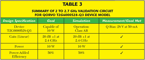
Table 3 and Figure 9 outline a third example, a 2 to 2.7 GHz design built by Qorvo producing 10 W, 50 percent efficiency and 20 dB gain with same device from the second PA example. Table 4 and Figure 10 show the details of the fourth PA validation circuit example using a model for the Qorvo T2G6003028-FS packaged product. This is a narrowband design centered at 5.8 GHz with 30 W of output power, while achieving 50 percent power-added efficiency and 14 dB gain. There is good agreement between simulation and measurement, except for a slight shift down in center frequency from the design target. A recent application note discusses the circuit level modeling process for this circuit in some detail, performed using Keysight ADS.8
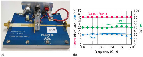
Figure 9 10 W, 2 to 2.7 GHz PA (a) with simulated vs. measured performance at 3 dB compression (b). Solid lines = simulation, symbols = measurement.
For all four of these designs, first pass design success was achieved thanks to the accuracy of the models used along with ADS simulations and optimizations of the circuits and element values prior to fabrication.
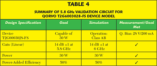

Figure 10 30 W, 5.8 GHz PA (a)8 with simulated vs. measured gain and output power (b) and power-added efficiency (c). Solid lines = simulation, symbols = measurement.
CONCLUSION
A productive collaboration between Qorvo and Modelithics has led to the advancement of an extensive library of GaN models for discrete die and packaged transistors. Each model is very well documented with extensive device level validations outlined in a model information datasheet. A series of power amplifier reference designs have been used to validate the utility and accuracy of the models for practical PA design. This work has demonstrated that the new paradigm in PA design is to start with sound device models and solid modeling of all passive networks with the goal of replacing “old school” bench tuning with simulation and optimization to enable a one-pass ‘simulate-build-test-done’ PA design process.
ACKNOWLEDGMENTS
The authors would like to thank the Modelithics engineering team for their hard work in developing and maintaining the Modelithics-Qorvo GaN library and the associated validations discussed in this application note. Thanks also to Richard Martin and Neil Craig of Qorvo for their enabling coordination of the collaboration leading to the described model library as part of the Modelithics Vendor Partner program.
References
- S. C. Cripps, “A Theory for the Prediction of GaAs Load-Pull Power Contours,” IEEE MTT-S International Microwave Symposium Digest, Vol. 1, May 1983, pp. 221–223.
- L. Dunleavy, C. Baylis II, W. Curtice and R. Connick, “Modeling GaN: Powerful But Challenging,” IEEE Microwave Magazine, Vol. 11, No. 6, October 2010, pp. 82–96.
- M. Golio, L.Dunleavy and T. Gneiting, “History and State-of-the-Art in Large Signal Modeling for RF/Microwave Power Amplifier Development,” IEEE MTT-S International Microwave Symposium Digest, May 2015, pp. 1–4.
- P. J. Tasker, “Practical Waveform Engineering,” IEEE Microwave. Magazine, Vol. 10, No. 7, December 2009, pp. 65–76.
- I. Angelov, H. Zirath and N. Rorsman, “A New Empirical Nonlinear Model for HEMT and MESFET Devices,” IEEE Transactions on Microwave Theory and Techniques, Vol. 40, No. 12, December 1992, pp. 2258–2266.
- S. C. Cripps, “RF Power Amplifiers for Wireless Communications,” 2nd Edition, Artech House, 2006.
- “Comprehensive Models for RLC Components to Accelerate PCB Designs,” Microwave Journal, Vol. 47, No. 5, May 2004.
- “Analysis of a 30 W Power Amplifier Utilizing Modelithics’ Triquint T2G6003028-FS Model in Agilent ADS,” Modelithics Application Note 49, Web. www.modelithics.com.
Contact Information
For information on accessing the Modelithics-Qorvo GaN Model Library visit www.modelithics.com/mvp/qorvo (free to Qorvo approved designers). Contact support@modelithics.com in case of any difficulties or questions about Library or PA validation circuits. For information about Modelithics CLR Library or Modelithics COMPLETE Library, contact Modelithics at sales@modelithics.com or visit www.modelithics.com.