
This article presents a new set of expressions for current and voltage in the continuous Class F-1 mode to produce a variable third harmonic impedance. The harmonic matching network (MN) in the conventional Class F-1 is adopted and placed in front of the fundamental MN to control the second and third harmonic impedances as well. The simplified real frequency technique (SRFT) algorithm is utilized to match the fundamental impedance over a wide band. A 10 W GaN HEMT device is used to design a continuous Class F-1 power amplifier. Greater than 71 percent drain efficiency is achieved from 2.1 to 2.4 GHz with a maximum efficiency of 84.3 percent at 2.3 GHz. The power amplifier can provide 39.7 to 40.8 dBm output power with greater than 10 dB saturated gain. For a 20 MHz OFDM signal with a peak-to-average power ratio (PAPR) of 8.4 dB, the adjacent channel leakage power ratio (ACLR) is below -50 dBc by employing digital predistortion (DPD), with an average output power of 31.2 dBm and 29.5 percent efficiency. For a 100 MHz, five carrier OFDM signal with a PAPR of 7 dB and an average output power of 32.8 dBm, an ACLR below -45 dBc can be achieved with the help of DPD; in this case, the efficiency is 39 percent. The continuous Class F-1 power amplifier has good linearity and is suitable for use in modern communication systems.
The power amplifier (PA) is a key element in wireless communication systems. Higher efficiency is always an important goal for PA designers, as high efficiency means less cost for cooling, system stability and energy conservation. Harmonically-tuned PAs such as Class F and inverse Class F (Class F-1),1,2 can offer high efficiency via non-overlapping voltage and current waveforms. For example, the Class F PA can offer high efficiency by controlling the first three harmonic impedances.3 Due to bandwidth limitations, however, they can hardly satisfy the wide band requirements of modern communication networks such as LTE-Advanced, which needs up to 100 MHz signal bandwidth.4
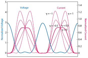
Figure 1 Voltage (normalized to Vdc) and current (normalized to Imax) waveforms of the continuous Class F-1 mode.
To address the narrow bandwidth of the Class F and Class F-1 modes, continuous Class F and continuous Class F-1 modes have been proposed.5,6 These continuous modes exhibit broadband characteristics while offering the same power and efficiency as conventional Class F and Class F-1. For continuous modes, the fundamental and second harmonic impedances are extended over wide ranges, providing a wider design space. Initially, the continuous mode was validated experimentally using the active load-pull measurement system developed at Cardiff University. In recent years, many physical continuous mode PAs have been realized and reported.7-11 All show high efficiency over a wide band; however, the harmonic impedances were not as well controlled as the theory showed.
Neither the continuous Class F nor the continuous Class F-1 theoretically relieves the third harmonic impedance condition, which cannot be realized in practical design. In this article, the expressions for voltage and current of the continuous Class F-1 mode are modifed to extend the range of the third harmonic and a method for matching with harmonic control is described. Both continuous wave and modulated signals are used to test PA performance.
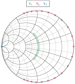
Figure 2 Admittances of the continuous Class F-1 mode.
CONVENTIONAL CONTINUOUS INVERSE CLASS F PA
To solve the narrowband problem for Class F and Class F-1 PAs, the continuous mode has been presented and researched in recent years.5,6,12 The continuous Class F-1 is one example. Its voltage and current waveforms are described by11

where Vdc is the drain operating voltage, Imax is the saturation current of the device, idc = 0.37, i1 = 0.43, and i3 = 0.06, with -1 ≤ Υ ≤ 1. Figure 1 shows the voltage and current waveforms.
The load impedance is11

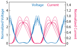
Figure 3 Modified voltage (normalized to Vdc) and current (normalized to Imax) waveforms of the continuous Class F-1 mode.
where the subscript n is the order of the harmonic component. We define Yopt in terms of the knee voltage Vknee and the quiescent bias current Iq as

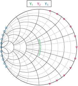
Figure 4 Admittances of the modified continuous Class F-1 mode.
Figure 2 shows these admittances on a Smith Chart.
MODIFIED CONTINUOUS INVERSE CLASS F PA
As shown in Figure 2, the continuous mode theoretically eliminates the restriction of impedance being a single point, expanding it over a wide range on the Smith Chart. This makes designing wideband PAs more feasible. However, there are two drawbacks. First, with variation of Υ, the current will exceed the maximum current of the device and current clipping will occur.13 Second, the third admittance of the continuous Class F-1 is just a single point.
Carrubba, et al.,14 proposed a set of voltage and current waveform formulations that allow reactive excursions of the third harmonic impedance of the continuous Class F PA. Similarly, new voltage and current waveforms of the continuous Class F-1 mode, are expressed as

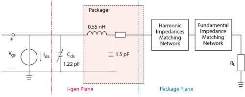
Figure 5 Output match of the continuous Class F-1 PA with approximated equivalent network of device output parasitics.
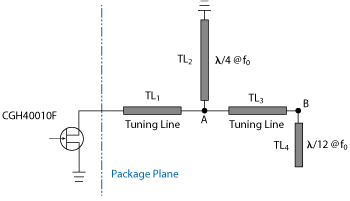
Figure 6 Harmonic matching network.
In order to eliminate current clipping, the current waveform should be modified so as not to exceed the maximum current, Imax The modified current from Equation 7 is

the new current stays below Imax with -1 ≤ γ ≤1 as shown in Figure 3. Using Equations 3, 6 and 8, the first three harmonic admittances are

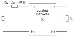
Figure 7 SRFT matching network.
Figure 4 shows the impedance condition for the modified continuous Class F-1 mode, which has a more flexible third harmonic impedance range compared to the conventional one.
DESIGN OF THE MODIFIED CONTINUOUS CLASS F-1 PA
The continuous Class F-1 mode theoretically provides high efficiency over a wide bandwidth, but it is difficult to control the fundamental, the second and the third harmonic impedances simultaneously. Some avoid this by matching the fundamental impedance first and then optimizing the matching network to keep away from the low efficiency regions of the second and the third harmonic impedances.7,8 In these designs, the harmonic impedances are not located in their theoretical regions — the harmonic impedances are matched before the fundamental impedance is matched.
GaN devices, having high breakdown voltages, are suitable for designing continuous Class F-1 PAs. The design implemented in this article uses a 10 W CGH40010F GaN HEMT, a packaged device from Cree. The entire output match is shown in Figure 5; the device package11 is also included.

Figure 8 Conversion from LC to transmission line network.
In order to control the harmonic impedances effectively, the harmonic MN is placed prior to the fundamental MN. The structure of the harmonic MN is illustrated in Figure 6.15 All of the transmission lines have the same characteristic impedance of 50 Ω.
The transmission line TL2 is a quarter-wave short-circuited stub, providing a short circuit condition to the second harmonic at point A. The effect from posterior circuits to the second harmonic impedance is eliminated. TL1 is a tuning line that transfers the short-circuit condition at point A to the open-circuit condition at the I-gen plane, together with the device output parasitics. At the third harmonic, TL4 provides a short-circuit condition at point B, while TL2 provides an open-circuit condition at point A. In this case, the transmission lines TL1 and TL3 together with the device parasitics present a short at the I-gen plane. Although the second and third harmonic impedances move from the open-circuit point and the short-circuit point, respectively, with the operational frequency deviating from the center frequency, f0, the excursion is acceptable in the modified continuous Class F-1 mode.
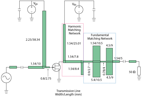
Figure 9 Schematic of the continuous Class F-1 PA.
To accomplish broadband matching, the SRFT algorithm is a good method for its simplicity, and it has been widely used in broadband PA design.8,16 This algorithm was first introduced by Yarman17 for solving the double-matching problem. In this work, it can be simplified by making the source impedance 50 Ω as shown in Figure 7, where ZL is frequency dependent complex impedance.
The S-parameters of the lossless network are

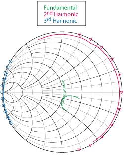
Figure 10 Admittances at the I-gen plane.
where k is the order of the zero of transmission at s = ∞, h(s) and g(s) are n order polynomials, with g(s) a strictly Hurwitz polynomial. h(s) and g(s) can be expressed as

where n is the number of elements in the lossless network. These two polynomials meet the requirement

Usually, an LC ladder network consisting of series inductors and shunt capacitors is used as a matching network. In this case, k is 0 and s = jω. The transducer power gain (TPG) can be expressed as

The nearer TPG approaches 1, the better the matching effectiveness.
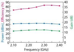
Figure 11 Simulated performance of the continuous Class F-1 PA.
Equations 12 and 13 show that the TPG function depends only on the coefficients of h(s). Optimization algorithms can be used to determine these optimal coefficients, and the polynomial is calculated using Equation 12. The normalized driving-point impedance is calculated with

then the Darlington procedure18 is used to produce the LC ladder network.
The resulting LC network must be converted to transmission lines in the practical PA design. The series inductor is replaced by a shorted transmission line with a high characteristic impedance,19 while the shunt capacitor is replaced by two shunt open-circuited stubs, as shown in Figure 8, where

This design, initially chooses Z1 as 75 Ω and Z2 as 25 Ω.
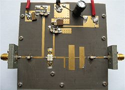
Figure 12 Fabricated power amplifier.
After designing the harmonic MN, the device model and the harmonic MN are used as a whole to perform load-pull in order to determine the optimal fundamental impedance. This is done in the AWR Design Environment using harmonic balance simulation. Then, SRFT is employed to design the fundamental MN. In this design, there are four elements in the LC ladder network.
The input match network is designed for high gain, adopting a simple form of a series high impedance transmission line and a short-circuited stub. After the input and output MNs are designed, optimization of the transmission line dimensions is necessary to achieve the best possible power, gain and efficiency over the entire bandwidth. The optimized PA is shown in Figure 9.
The frequency band is 2.1 to 2.4 GHz. The fundamental, second and third harmonic admittances at the intrinsic I-gen plane are shown in Figure 10. The figure shows they are well controlled. High efficiency is achieved across the band, as shown by the simulated performance in Figure 11.
FABRICATION AND MEASUREMENT
The PA is implemented with a Cree CGH40010F GaN HEMT mounted on a Taconic RF35 substrate with permittivity of 2.2 and thickness of 20 mils (see Figure 12). The drain bias is 28 V, the gate bias is -3 V and the PA draws a quiescent current of 30 mA.
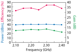
Figure 13 Measured performance of the continuous Class F-1 PA.
A single tone continuous wave signal swept from 2.1 to 2.4 GHz with 50 MHz spacing is used for the initial evaluation. Measured performance over the entire bandwidth is shown in Figure 13. The drain efficiency is greater than 71 percent, with a maximum efficiency of 84.3 percent at 2.3 GHz. Output power is 39.7 to 40.8 dBm, and the saturation gain is 10.4 to 13.3 dB.
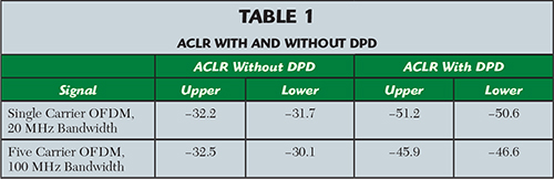
Two OFDM signals with different bandwidths are used to replicate actual communication systems. The first is a 20 MHz OFDM signal with a PAPR of 8.4 dB and a center frequency of 2.15 GHz. For an average output power of 31.2 dBm, the ACLR is -31.7 dBc (at -20 MHz) and -32.2 dBc (at +20 MHz). To satisfy communication system requirements, linearization is necessary. With DPD, the ACLR is improved to -50.6 dBc (at -20 MHz) and -51.2 dBc (at +20 MHz), as shown in Table 1. In this case, the average efficiency is 29.5 percent. The output power spectrum with and without DPD is shown in Figure 14a. To test the performance of PA in broadband systems, the second modulated signal is a 100 MHz OFDM signal with a PAPR of 7 dB. When the average output power is 32.8 dBm with 38 percent drain efficiency, ACLR with DPD is improved to -45.9 dBc (at +100 MHz) and -46.6 dBc (at -100 MHz) from -32.5 dBc (at +100 MHz) and -30.1 dBc (at -100 MHz), as listed in Table 1. The PA meets modern communication systems requirements. The output power spectrum is displayed in Figure 14b.
CONCLUSION
Equations for the continuous Class-F-1 mode are modified to extend the range of the third harmonic impedance. The harmonic MN is placed in front of the fundamental MN to achieve better harmonic matching. The harmonic MN is that of a conventional Class-F-1 amplifier, while the fundamental MN is synthesized using the SRFT algorithm. The fabricated PA has a drain efficiency of greater than 71 percent from 2.1 to 2.4 GHz, with a maximum efficiency of 84.3 percent. It produces about
10 W output power with greater than 10 dB gain over the band. Two OFDM signals with different bandwidths are used to evaluate the performance for communication systems. DPD is used for linearization. For a 20 MHz single carrier signal with a PAPR of 8.4 dB, ACLR is below -50 dBc for the upper and lower bandwidth, while the average output power is 31.2 dBm with 29.5 percent drain efficiency. For a 100 MHz, five carrier signal with a PAPR of 7 dB, when the output power is 32.8 dBm and the efficiency is 38 percent, the ACLR is below -45 dBc. The continuous Class-F-1 PA has good linearity, suitable for use in modern wideband communication systems.
ACKNOWLEDGMENT
The authors would like to acknowledge Dr. Yinjin Sun and Dr. Fan Meng for providing their research group’s DPD platform for linearization.
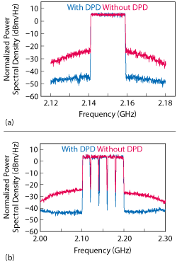
Figure 14 Measured output spectrum with and without DPD for 20 MHz, single carrier, OFDM signal (a) and 100 MHz, five carrier, OFDM signal (b).
References
- Y. Woo, Y. Yang and B. Kim, “Analysis and Experiments for High-Efficiency Class-F and Inverse Class-F Power Amplifiers,” IEEE Transactions on Microwave Theory and Techniques, Vol. 54, No. 5, May 2006, pp. 1969–1974.
- J. Kim, G. Jo, J. Oh, Y. Kim, K. Lee and J. Jung, “Modeling and Design Methodology of High-Efficiency Class-F and Class-F-1 Power Amplifiers,” IEEE Transactions on Microwave Theory and Techniques, Vol. 59, No. 1, January 2011, pp. 153–165.
- F. H. Raab, “Maximum Efficiency and Output of Class-F Power Amplifiers,” IEEE Transactions on Microwave Theory and Techniques, Vol. 49, No. 6, June 2001, pp. 1162–1166.
- J. Xia, X. Zhu, L. Zhang, J. Zhai and Y. Sun, “High-Efficiency GaN Doherty Power Amplifier for 100 MHz LTE-Advanced Application Based on Modified Load Modulation Network,” IEEE Transactions on Microwave Theory and Techniques, Vol. 61, No. 8, August 2013, pp. 2911–2921.
- V. Carrubba, A. L. Clarke, M. Akmal, J. Lees, J. Benedikt, P. J. Tasker and S. C. Cripps, “The Continuous Class-F Mode Power Amplifier,” European Microwave Conference, September 2010, pp. 432–435.
- V. Carrubba, A. L. Clarke, M. Akmal, Z. Yusoff, J. Lees, J. Benedikt, S. C. Cripps and P. J. Tasker, “Exploring the Design Space for Broadband PAs Using the Novel Continuous Inverse Class-F Mode,” EuropeanMicrowave Conference, October 2011, pp. 10–13.
- B. Merrick, J. King and T. J. Brazil, “A Simplified Procedure for the Design of Continuous Class-F Power Amplifiers,” European Microwave Conference, October 2013, pp. 1479–1482.
- N. Tuffy, L. Guan, A. Zhu and T. J. Brazil, “A Simplified Broadband Design Methodology for Linearized High-Efficiency Continuous Class-F Power Amplifiers,” IEEE Transactions on Microwave Theory and Techniques, Vol. 60, No. 6, June 2012, pp. 1952–1963.
- V. Carrubba, J. Lees, J. Benedikt, P. J. Tasker and S. C. Cripps, “A Novel Highly Efficient Broadband Continuous Class-F RFPA Delivering 74 Percent Average Efficiency for an Octave Bandwidth,” IEEE MTT-S International Symposium Digest, June 2011, pp. 1–4.
- R. Tong, S. He, B. Zhang, Z. Jiang, X. Hou and F. You, “A Novel Topology of Matching Network for Realizing Broadband High Efficiency Continuous Class-F Power Amplifiers,” European Microwave Conference, October 2013, pp. 1475–1468.
- K. Chen and D. Peroulis, “Design of Broadband Highly Efficient Harmonic-Tuned Power Amplifier Using In-Band Continuous Class-F-1/F Mode Transferring,” IEEE Transactions on Microwave Theory and Techniques, Vol. 60, No. 12, December 2012, pp. 4107–4166.
- S. C. Cripps, P. J. Tasker, A. L. Clarke, J. Lees and J. Benedikt, “On the Continuity of High Efficiency Modes in Linear RF Power Amplifiers,” IEEE Microwave and Wireless Components Letters, Vol. 19, No. 10, October 2009, pp. 665–667.
- S. C. Cripps, “RF Power Amplifiers for Wireless Communications,” Artech HouseNorwood, Mass., 2006.
- V. Carrubba, R. Quay, M. Schlechtweg, O. Ambacher, M. Akmal, J. Lees, J, Benedikt, P. J. Tasker and S. C. Cripps, “Continuous Class-F3 Power Amplifier Mode Varying Simultaneously First 3 Harmonic Impedances,” IEEE MTT-S Microwave Symposium Digest, June 2012, pp. 1–3.
- A. Grebennikov, “High-Efficiency Transmission-Line Inverse Class F Power Amplifier for Active Antenna Arrays,” Asia–Pacific Microwave Conference, December 2009, pp. 317–320.
- D. Y. –T. Wu, F. Mkadem and S. Boumaiza, “Design of a Broadband and Highly Efficient 45 W GaN Power Amplifier via Simplified Real Frequency Technique,” IEEE MTT-S International Microwave Symposium Digest, June 2010, pp. 1090–1093.
- B. S. Yarman and H. J. Carlin, “A Simplified ‘Real Frequency’ Technique Applied to Broadband Multistage Microwave Amplifiers,” IEEE Transactons on Microwave Theory and Techniques, Vol. 30, No. 12, December 1982, pp. 2216–2222.
- B. S. Yarman, “Design of Ultra Wideband Power Transfer Networks,” Wiley, New York, 2010.
- D. M. Pozar, “Microwave Engineering,” Wiley, New York, 2010.