
Editor’s Note: As the Internet of Things (IoT) becomes a growing trend of design and development, we asked some leading software EDA companies to provide practical examples of how their tools are enabling IoT design. These examples range from wearable devices to 5G, medical and industrial applications.
Supporting the IoT Design Chain
ANSYS
Canonsburg, Pa.
IoT will be developed on such a large engineering scale across so many industries (medical, transportation, industrial, etc.), that it will transform the electronics industry, revolutionize the RF/microwave component supply chain and place new demands on design tools, workflows and skill sets. Estimates call for 200 billion smart devices by 2020 with devices outnumbering people by a ratio of 26 to one. The IoT ecosystem will enable massive data collection (sensing), connectivity M2M (machine to machine) and H2M (human to machine) on a host of platforms (wearables, connected homes, cars, cities, medical, industry, etc.) supported by cloud infrastructure.
Furthermore, power consumption, data security and communication standards compliance will be critical design requirements for connected applications. Striking an optimal balance between power efficiency, antenna integration and performance, security and cost is a key design challenge faced by engineers developing IoT devices and infrastructure. Therefore, design tools must help engineers develop robust, high-fidelity communications, power conservative mixed signal-processing and cost optimized electronics. These capabilities have been the focus of ANSYS’ software development and strategic acquisitions, leading to a product portfolio and roadmap that is uniquely aligned with a complex design chain developing the full range of integrated circuits (IC), sensors, antennas and embedded software that will define IoT.
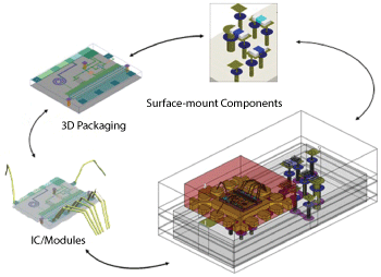
Figure 1 System workflow to address complete design cycle.
Since the industry’s inception, market leaders have relied on simulation-driven product development to launch their devices quickly, cost-effectively and with a high degree of confidence that they will perform as expected. Moving forward, engineering teams will need to adopt new technologies more rapidly than ever before. Technologies adopted for IoT will be developed and integrated with software tools that accurately address real-world physical design, offering solver technologies with the speed and capacity to simulate smart devices in their operating environment using a workflow that optimizes engineering productivity.
With smaller, portable devices operating at low power, designing components in isolation is no longer a valid approach. Engineers cannot work from the abstract of a schematic for individual components; they must consider the geometry of the actual device to include all of the physical effects. This means being able to visualize the entire physical design, insert appropriate components (such as surface-mount devices, connectors and ICs), and run both frequency and time domain simulations with all electromagnetic and thermal/mechanical effects included. ANSYS multiphysics products support virtual prototyping through simulation of the electrical, thermal (with ANSYS Icepak) and mechanical behavior of components based on geometries and materials defined by the engineer. Structures can range from a miniaturized, embedded antenna array to stacked die in electronic package on a complex PCB.
ANSYS addresses electronic design from the chip to the package and board, through the mobile/base station antennas and over-the-air – from baseband to RF. IoT electronics will require a chip–package–system workflow coupled to multi-physics for thermal and mechanical stress analyses (see Figure 1). The ANSYS CPS workflow includes Chip Power Model (CPM), a compact SPICE-correlated model of the full-chip power delivery network. CPM comprises spatial and temporal switching current profile as well as nonlinear on-chip devices to accurately represent chip behavior for package and PCB simulation. The workflow employs advanced meshing and multi-CPU solver technologies to rigorously solve Maxwell’s equations and generate accurate broadband models of the package and PCB. This approach enables engineers to identify and address root causes of signal integrity and power integrity issues, balancing the lower operating voltages needed to conserve power with the consistency and reliability required to eliminate device failures.
Design Examples
Using simulation to achieve extremely low power, compact size and comprehensive connectivity is exemplified in Atmel’s IEEE 802.11 b/g/n IoT network controller SoC and family of ARM Cortex-M0+ MCUs. The design team leveraged ANSYS HFSS, ANSYS RedHawk and ANSYS Totem to design and validate these complex SoCs and platforms used across multiple IoT application segments. These simulation solutions enabled the company to meet stringent power/performance requirements, ensure reliable operations across a wide-range of frequencies and deliver products with tight time-to-market constraints.
ANSYS software development is focused on several notable innovations that allow engineers to leverage component level IP that can be incorporated into simulation models and combined hierarchically into complex systems with an accuracy previously reserved for design verification. Moving to this level of simulation fidelity earlier in the design process saves significant time and costs, but does require more computing power. High performance computing (HPC) delivers this computational power for HFSS simulations by leveraging more nodes of a compute cluster or cloud environment to accelerate design efforts through combined distribution of design parameters, frequencies and multi-core/multi-domain EM solvers. With several notable features, such as distributed direct matrix and domain solvers, HPC is becoming widely adopted among HFSS users.
The exchange of design information between engineering disciplines (i.e., electrical and mechanical) and across organizations (i.e., vendor and OEM) will be one of the major challenges for IoT. Along with simulation run times, design entry (model set-up) and workflows between tools play a major role in defining engineering productivity and limiting design exploration. In 2015, HFSS became fully integrated with the company’s circuit and system simulation tools in the new ANSYS Electronics Desktop, a single-window, highly integrated interface that provides a seamless working environment to maximize productivity and to ensure users are following simulation best practices. In addition, the ANSYS Electronics Desktop features a 3D EM (electromagnetic) component library.
The 3D EM library, which both engineers and CAD support teams can use, can be coupled with IP (intellectual property) protecting encryption to share HFSS components between design teams and across high-frequency supply chains to expedite communication system integration, a critical factor in support of a broad IoT eco-system. Users can create 3D components and integrate them into larger electronic assemblies. Simulation-ready 3D components stored in library files can be added to larger system designs without requiring the user to apply excitations, boundary conditions and material properties.
The potential impact 3D EM components will have on the IoT design chain is perhaps most evident in the case of antenna design and placement. Embedded antennas in wearable devices often radiate in all directions with considerable energy being absorbed by the body. Using HFSS and Optimetrics, engineers at Vortis Technology Inc. were able to explore more design scenarios in the development of their micro array antenna using interferometry to reshape the RF energy fields and reduce the unwanted RF signal strength toward the user while enhancing the emissions toward the receiving sites. Design exploration through parametric modeling and optimization automates the design process, while the analytic derivative can extract design sensitivity from a single simulation. Designers at Vortis were able to determine the optimum placement of the two antennas phased 180 degrees in order to create a null of energy against the body while the signals enhance each other in the desired direction. The result was a 10 fold drop in energy toward the body and an equal enhancement in the radiated far fields thereby improving efficiency and extending battery life. The encrypted antenna could then be distributed in a component library to IoT mobile device manufacturers for further design and integration into their platform.
IoT models (mechanical designs) will come from many sources. To accelerate model development, ANSYS simulation tools can import electronic CAD (ECAD) and mechanical CAD (MCAD) data from a variety of sources, streamlining the transfer of design databases from EDA layout tools offered by Altium, Cadence, Mentor Graphics and Zuken or 3-D geometries from mechanical CAD (MCAD) packages using common file formats, such as IGES, STEP, ACIS and Parasolid. With ANSYS SpaceClaim Direct Modeler, designers can quickly prepare geometries from these CAD systems for simulation by cleaning up and simplifying geometries, adding parameters, and a host of pre-simulation model prepping operations. The imported CAD model becomes completely dynamic, allowing designers to move, stretch, add and remove with mouse movements. All changes to the CAD model occur in real-time on the screen for instant feedback, ready for export into HFSS and reducing labor-intensive model prep from weeks down to hours.
Simulation of Antennas for Wearable IoT Devices
CST – Computer Simulation Technology
Darmstadt, Germany
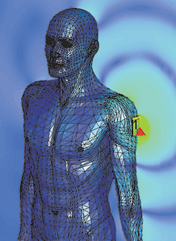
Figure 2 Electric field around a flexible worn slot antenna.
The whole idea of the Internet of Things is to network together physical objects so that they can exchange data with each other, with the operator and with the manufacturer. This improves the value of the devices and the quality of the service. In order to monitor and affect the surroundings, the “things” containing sensors, controllers and actuators need to be connected together.
The proliferation of smart devices and installation challenges of cables mean that the majority of IoT devices are designed to operate wirelessly. Electromagnetic simulation allows the antennas that connect these devices to be modeled in a realistic environment in order to analyze installed performance, with the aim of improving the reliability and efficiency of the IoT.
New antenna technologies require multiple antennas (sometimes with MIMO antenna diversity) operating in multiple frequency bands within a small physical profile. Antenna placement plays a significant role in determining the performance of an antenna, and can also lead to potential co-site interference effects between systems.
Wearable antennas, as used in body-area networks, pose a special challenge in this regard. Currently, the most familiar commercial application for wearable technology is the rapidly-growing market for smart watches and fitness trackers. However, the antennas also have considerable potential to allow better diagnostic technology for medical patients, and to allow rescue personnel and other workers in dangerous environments to be monitored in real-time.
These antenna requirements are stringent: they have to achieve a given performance with severe restrictions on form factor (low profile, lightweight, integrated into clothing or worn devices) and are installed in a challenging environment next to a large volume of high permittivity lossy material – the human body. In addition, there are legal constraints regarding human exposure to EM fields that need to be considered.
Because IoT devices often need to be small and low cost, integrated printed antennas offer a considerable advantage over off-the-shelf designs. Antenna Magus and CST STUDIO SUITE make it possible to quickly synthesize and optimize printed antennas on a densely populated PCB.
Design Example
Simulating the device on a human body model offers a far more accurate picture of real-world than simply considering the antenna’s performance in isolation. Other components within the device as well as the body itself will absorb or reflect power (shown in Figure 2), and changes to the antenna itself will also affect its efficiency and directivity. This is especially important for flexible antennas which can be integrated into clothing, including state-of-the-art woven antennas. Bending, twisting or stretching the antenna changes its properties, and for applications where reliability is crucial, it is vital to ensure that the antenna performs within specifications for all plausible configurations. With virtual prototypes, antenna performance can be calculated and the design optimized to counteract detuning effects.
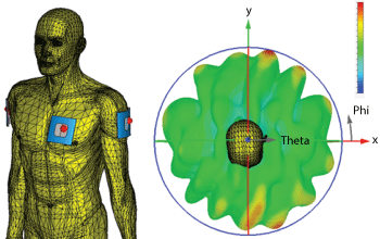
Figure 3 Four flexible antennas combined into a MIMO body-worn system (a) and realized gain at 2.4 GHz with all antennas excited simultaneously (b).
Another consideration – one that is vital for regulatory approval – is specific absorption rate (SAR). This is a measure of how much energy tissues within the body absorb, which is very difficult to measure in vivo. The human body is not homogeneous, and the different tissues that comprise it often have very different properties – muscle for example has rather different electrical and thermal properties to bone. Simulating the SAR – and finding the worst-case scenario – allows engineers to calculate how much power can be safely input to the antenna and can reduce the risk of failing to meet regulatory limits at the expensive physical prototyping stage.
A realistic SAR calculation requires a detailed heterogeneous body model – for example, a voxel model or a specially constructed CAD model – that includes all the relevant structures inside the body. CST STUDIO SUITE includes a toolbox of SAR calculation techniques that can calculate the power absorbed both at individual points within the body and averaged over volumes of tissue. Both the current standard, IEEE C95.3, and the upcoming standard IEEE/IEC 62704-1, are supported, and CST is involved in the ongoing development of SAR standards.
In order to improve connectivity in complex environments, MIMO systems and beam-steering are increasingly used in portable devices. A benefit of MIMO is that it can offer improved performance in complex multi-path environments – for example, built-up areas. Multi-path signal transmission may lead to destructive signal overlay, resulting in local deep dips in an effect called Rayleigh fading. Using multiple antennas (antenna diversity) allows this fading to be reduced.
CST STUDIO SUITE has several built in post-processing options to evaluate the potential MIMO performance which can calculate the envelope correlation (including spatial power weighting functions), diversity gain and multiplexing efficiency. Figure 3 shows the antennas for a wearable device with MIMO – there are four antennas to cover the shadowed areas of the body, and each one is locally conformal. Because each flexible antenna is warped differently, and because the body beneath is lossy, the antennas individually have variable performance (the most distorted antennas on the arms have a frequency shift of about 50 MHz relative to the least distorted). Nevertheless, good performance is achieved using MIMO, with a good pattern and spatial diversity, a low correlation coefficient and a good multiplexing efficiency.
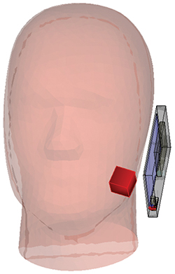
Figure 4 Localized peak SAR when using phone near head.
Simulation is an essential tool in the design flow for the realization of IoT devices. Different antennas at different frequencies can be integrated into a single compact device, and their performance analyzed in a realistic environment. Human body models can be integrated into the simulation model, and important biological results such the SAR can be calculated. The performance of the antennas integrated into a larger system can also be calculated, taking into account the MIMO principles of modern communications. Together, all of these features allow simulation to be used at any stage of the design process from a single integrated environment.
5G and IoT Development Flexibility
FEKO (Altair Development)
South Africa
Along with the advancements in mobile communications technologies, there is a tremendous development in the mobile handset hardware over the years, and mobile phones have evolved from the “brick” model to the present-day “slick” models. This evolutionary process has also brought significant changes to the antennas that go into these mobile handsets. As a result, antenna designers have moved from the simple monopole and printed inverted-F antennas to complex electrically small antennas.
FEKO’s Method of Moments (MoM) and its extensions to solve dielectrics are well suited to the design and optimization of mobile antennas. Planar Green’s functions, the Surface Equivalence Principle (SEP) and Volume Equivalence Principle (VEP) extensions to the MoM are all available in FEKO, providing designers with simulation methods to solve a wide range of different mobile antenna topologies.
The Finite Element Method (FEM) has also been fully hybridized with the MoM in FEKO, providing users with the ability to blend the strengths of these simulation methods to solve complex dielectric antennas. The FEM-MoM hybrid also provides users with the ability to estimate SAR for new devices in close proximity to humans (see Figure 4). Localized peak SAR (1 and 10 g cubes) or whole body average SAR levels can easily be computed. In situations where the entire body or other electrically large objects have to be included in simulations of mobile antennas, the Multilevel Fast Multipole Method (MLFMM) may be used to accelerate the solutions methods that have already been mentioned here.
FEKO also incorporates a technique called Characteristic Mode Analysis (CMA) that helps designers follow a systematic, intelligent approach rather than a brute force method, by looking at the eigen-value spectrum and the eigen-vector distribution. CMA is used to design a mobile antenna operating in the LTE 1.8 GHz band (see Figure 5). A predefined surface area is assumed on which the antenna will be etched, in this case a curved metal sheet on the outer edge of the PCB. CMA is then used to calculate the modal currents on the surface for the dominant modes at 1.8 GHz. The advantage of this approach is that it is more intuitive than standard optimization algorithms and therefore the optimum design requirements can be met in less iterations.
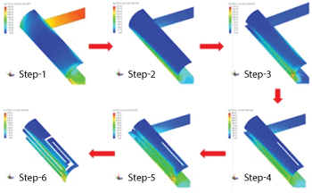
Figure 5 LTE antenna is designed by modifying the metal sheet systematically based on the modal current distribution.
CMA can also be used to find the optimum placement of the battery connector with respect to the antenna and the spacing of the battery from the PCB. The combined performance including display frame and battery are shown previously, compared to the original antenna and PCB only. An improvement of 5 percent in radiation, 5 dB in coupling and up to 1 dB in MEG where achieved.
The major advantages that CMA offered in this study were two-fold: namely the CMA simulations are fast (on the order of a few minutes) and bring valuable insight through the modal currents, which helped improve an antenna design during the integration process.
Design Examples
Examples show application of advance simulation technologies in FEKO for 4G/LTE applications, but they can also be effectively incorporated for 5G antenna designs for mobile devices and base stations.
One of the main aspects of IoT is the requirement for key components to enable communications between devices and objects. Objects need to be augmented with an Auto-ID technology, typically an RFID tag, so that each object is uniquely identifiable. Also, an RFID tag allows the object to wirelessly communicate certain types of information, which leads us to another requirement – the ability to monitor data. Truly smart objects will be embedded with both an RFID tag and a sensor to measure data. The sensor may capture fluctuations in the surrounding temperature, changes in quantity, or other types of information. FEKO is being used effectively in characterizing RFID tags, optimization of RFID tag placement as well as the operating environment within which the reader antenna communicates with the tag (see Figure 6).

Figure 6 Excalibur tag antenna current distribution and radiation pattern (a) and surface current distribution and radiation pattern of tag antenna on a pallet of metal canisters (b).
FEKO not only offers the numerical methods such as MoM, MLFMM, FEM, FDTD, etc., but also asymptotic, ray-based method such as the uniform theory of diffraction or ray launching geometrical optics (shooting and bouncing rays) that are used for electrically extremely large RFID problems such as long distance indoor propagation (see Figure 7). On the other hand, for electrically small but dielectrically complex problems, such as tag-reader interaction in the presence of the human body, the finite element method (FEM) or Finite Difference Time Domain (FDTD) can be employed. The FEM can either be used by itself or in hybrid coupling with the MoM (e.g., the reader antenna is modeled with the MoM, while the human body is being modeled with the FEM in order to combine the strong points of the two methods). FEKO, with its advanced and comprehensive computational techniques, is playing a major role in 5G systems as well as Internet of Things.
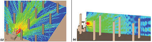
Figure 7 Near field pattern in a warehouse environment from RFID reader antenna mounted on a forklift (20 dB visualization range) (a) and vertical near field cut in front of a RFID reader antenna (30 dB visualization range) (b).
Enabling 5G and IoT Development
Keysight EEsof EDA
Santa Rosa, Calif.
Over the next five years, 5G and IoT design engineers will be facing familiar trends: increasing design size, higher integration and design complexity, movement from single IC designs to multichip modules, integration of multiple technologies (e.g., GaAs, GaN, SiGe/Si/SOI and CMOS), and more challenging standard specifications. Smaller design teams with tighter budgets will also continue to be a key trend, and this will drive efficiency improvement initiatives designed to improve design flow efficiency.
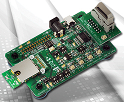
Figure 8 Renesas’ Bluetooth Smart Wireless Solution will enable designers to more easily develop Bluetooth Smart applications for the IoT.
While these trends bring a number of key benefits, they are also forcing 5G and IoT design engineers to face new challenges, many of which are an extension of those the industry has been working to address and solve over the last 10 years. Some of the key challenges include maximizing power efficiency, managing electro-thermal effects and dealing with the increasing circuit simulation issues that come from more complex designs, while simultaneously handling the increased electromagnetic coupling that arises from more compact designs. Other challenges include integration, evaluating and choosing the “right” technology mix, and verifying performance to industry standard specifications across a wide frequency spectrum.
To stay at the forefront of these trends and overcome these challenges, today’s design engineers require flexible and powerful design solutions that keep pace with emerging trends and standards. Keysight EDA focuses on solving communication system design challenges, especially IC and PCB design and simulation of applications including 5G and 802.11xx wireless networking, as well as Bluetooth Low Energy (BLE), ZigBee and Wi-SUN for the IoT. Keysight’s customers are leading the industry with their 5G and IoT products, and they have relied on Keysight EDA software to get them there.
Design Examples
Renesas Electronics: BLE Smart Wireless Solution for IoT Applications:
Many IoT applications require small, battery-powered devices intended to operate over extended periods of time—for months or even years on just a button power cell. As a result, minimized power consumption is a key design constraint for IoT applications.
Renesas recently announced a new technology and group of microcontrollers that integrate a BLE RF transceiver capable of operating up to two years or more on a CR2032 button cell. The design utilizes an integrated Tx/Rx switch, DC/DC converter and matching network/filter reuse to reduce chip size and power consumption. High efficiency DC/DC converters typically require fast switching rates and compact silicon spirals, which produce RF frequency components and undesired electromagnetic effects.
Hisayasu Sato, Renesas design team manager and Keysight Certified Expert, successfully designed the transceiver in a single design iteration using Keysight GoldenGate Silicon RFIC and Momentum simulation software. Boasting the industry’s lowest current drain, the transceiver will serve as a core technology for short-distance wireless communication in wearable devices and other IoT applications. This enabled Renesas to accelerate its use of embedded devices in IoT applications and recently led to its release of the new RL78/G1D microcontrollers (see Figure 8).
Plextek RF Integration: 28 GHz, 4-channel, Phase Adjustable PA for 5G:
5G wireless is expected to give users the perception of near infinite capacity for “everything, everywhere and always connected.” To achieve this vision, devices will require significantly faster data rates and operation at mmWave frequencies with sufficient bandwidth. Signal propagation at mmWave; however, is much more challenging than at typical mobile wireless frequencies.
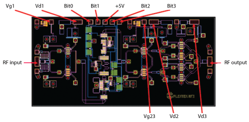
Figure 9 Layout of one channel of the Plextek RF Integration transmitter IC modeled in ADS.
To address this challenge, Stuart Glynn and Liam Devlin, CEO, Plextek RF Integration and Keysight Certified Expert, used Keysight’s Advanced Design System (ADS) software to develop an innovative 4-channel, 28 GHz, 5G phase adjustable PA IC design for use in 5G radio front-ends (see Figure 9). It was designed using a commercially available 0.15-µm GaAs PHEMT process and is intended to be housed in a low cost SMT package suitable for volume production. The IC can be used in either 5G mobile devices or base stations.
What makes the Plextek RF Integration IC unique is that each of its channels has a PA with an integral 4-bit, digitally controlled phase shifter, which provides a compact means of beam steering. Innovative components like this are critical to enabling the design of hardware suitable for mmWave frequencies with sufficient bandwidth.
As 5G wireless communication systems and the IoT continue to evolve, EDA tools will be crucial to advancing their ecosystems and transforming the promise of these industries into reality. Renesas and Plextek RF Integration are just two examples of leading-edge companies that have successfully used Keysight EDA’s solutions for 5G and IoT development. In addition to supporting its customers’ efforts, Keysight works closely with industry consortia, partner companies and academia. Plus, its R&D and application engineers—industry experts in their own right—play a critical role in developing the design software, bench instrumentation and manufacturing solutions to advance 5G and other emerging standards, as well as the IoT. It is this combination of leadership, application expertise and industry leading design tools that is enabling Keysight customers to solve even their most difficult design challenge.
Is the IIoT (Industrial IoT) Waiting on 5G?
NI, Austin, TX
The introduction of highly functional smart devices, such as the Apple iPhone and Android-powered devices, along with all of those cool apps has ignited the global demand for wireless data, and it has no indication of slowing down anytime soon. Mobile broadband data’s impact on our lives is unquestioned, yet faster data is just part of the larger picture. Applying reliable wireless service to industries such as transportation, construction, manufacturing, medicine and healthcare, and energy and smart grid can spur unprecedented economic growth. For example, 85 percent of the billions of embedded devices sold in 2014 were not connected to a network. But what if they were? Analysts predict that global networks must accommodate over 50 billion embedded devices by 2020. A collection of low power sensors connected to the Internet forms the foundation of the IoT. Many of these devices will be autonomous, embedded units powered by batteries or by small solar panels. Defining 5G networks has created a lot of excitement, and much of that attention has centered on faster data. However, 5G has a broader agenda. In addition to faster data, 5G will accommodate significantly more connected users and devices (100× or more) and will aim to address the challenge of network latency. Solving these less publicized challenges is the key to unlocking the IoT’s enormous potential.
IoT devices may not need the high data rates of today’s smartphones or tablets, but many IoT applications require faster and more deterministic response times to expand the IoT’s reach—from transforming older localized applications to using connected apps for creating new applications. Latency or network response time has not been a priority for standardization bodies such as the 3GPP or 802.11 because these entities have primarily focused on the increase in data rates. Consequently, latency in our current networks is unpredictable and nondeterministic, and can span from milliseconds to several seconds. This unpredictability is a nonstarter for many commercial entities looking for ways to use the network for remote access and control.
Earlier cellular networks, where voice was the dominant (or rather the only) application, required a latency that was just good enough to satisfy the listener. The human ear can discern sounds on the order of 100 ms. More sensitive than the ear, the human eye perceives visual discontinuities on the order of 10 ms, which is a useful metric for multimedia applications. Enabling the tactile Internet or considering touch requires much more stringent latency (less than 1 ms) because human touch is more discernible than either the eye or ear.
Design Examples
These examples outline the use cases at a crude level between network responsiveness and human perception whether considering sight, sound or touch. Applications that involve machines talking to machines require factoring in additional application sets: monitoring and control.
The two types of “monitoring” IoT use cases are:
- Human eye/visual
- Sensor logging—storing video or sensor data for later retrieval and review
Human eye/visual IoT monitoring/surveillance applications require latency requirements similar to those for human visual perception—on the order of tens of milliseconds (that is, the delivering mechanism can be the same, and the requirements must scale up or down with the applications). Sensor logging latency requirements can actually vary quite dramatically depending on the application and the deployed sensor capabilities. To illustrate this point, consider the rather mundane task of measuring temperature. Temperature sensors are used extensively in a variety of applications. If the sensor measures the ambient temperature, then the latency can be on the order of seconds, hours or even days as temperature changes because of climate conditions, which tend to vary over a wider time constant. We see applications like this today that are quite functional. Conversely, a sensor measuring the temperature of a chemical pour or mixing process might need to trigger an action if the temperature rises above a certain threshold to avoid damaging the end product or for safety reasons. This type of monitoring and economic benefit is directly tied to the capabilities of the network and is possible in localized proprietary implementations. This example introduces the concept of control that encompasses a round-trip response time for both uplink and downlink.
This type of control application cannot be performed with today’s networks because service operators cannot guarantee a minimum latency specification (and for the most part, the latency may be out of their control). The holy grail of 5G networks in terms of latency is to provide industries with predictable or deterministic latency response that is ideally in the submillisecond range. If service operators can deliver predictable network response, perhaps even for a designated geographic region, then companies can develop viable businesses.
The concept of “control” over a cellular network is radical. Combining control with the computational and storage power of the cloud promises to improve our everyday lives and spur economic growth. To be clear, “remote control” in this context refers to software running in the cloud, monitoring sensor data or video, and controlling processes deployed at a remote location—perhaps the control software resides in the cloud. Examples include factory automation/smart factories, traffic control/smart cities, smart grid/energy conservation, and healthcare monitoring and medicine disbursement. In aggregate, these ideas form the Industrial Internet of Things (IIoT). IIoT applications change the control paradigm; rather than discretely duplicating a particular control process a million times around the world, 5G networks can make the IIoT possible by delivering a consolidated control experience that reduces costs, improves quality, increases performance, and spawns new industries.
NI is working with researchers today to create 5G networks capable of supporting the IoT infrastructure necessary to drive the broader agenda. There are several examples of 5G technologies researched today that hold much promise. An example of a promising 5G candidate technology is mmWave. Despite efforts by governments around the world to reallocate spectrum, free spectrum below 6 GHz remains scarce. However, spectrum in the mmWave frequency is plentiful. To simplify, more spectrum equates to more capacity and more bandwidth per device. NI has been closely collaborating with researchers at Nokia Networks to prototype a mobile access networks at 73 GHz. Through this collaboration, Nokia and NI were able to publicly demonstrate the world’s first 10 Gbps mobile access link last April at the Brooklyn 5G Summit. Breakthroughs such as the Brooklyn 5G Summit demonstration hint that the 5G networks capable of providing a robust IoT infrastructure may not be that far away.