
This article describes the design of a 2.12 GHz Class F transmitter power amplifier (PA) using Cree’s CGH40010 GaN HEMT. Input and output matching networks are designed to approximate the fundamental and second harmonic impedances obtained in source and load pull simulations. It achieves both high efficiency and excellent linearity by employing the digital predistortion (DPD) technique. Measurements using continuous wave (CW) signals demonstrate a high power-added efficiency (PAE) of 75.2 percent at the maximum output power of 39.4 dBm. For a 20 MHz 4-carrier Wideband Code Division Multiple Access (WCDMA) excitation signal with 7.1 dB peak-to-average power ratio (PAPR), adjacent channel power ratios (ACPR) of the PA are –28.3 and –27.5 dBc at an average output power of 33.3 dBm. This is improved to –51.9 and –54.0 dBc after DPD. For a 20 MHz Long Term Evolution (LTE) signal with 6.6 dB PAPR, ACPR of the designed PA below –53 dBc is achieved after DPD at the same average output power. Drain efficiency (DE) of the PA is 37.8 percent with an average output power of 33.3 dBm.
In order to obtain high spectral efficiency and throughput in modern wireless communication systems, complex modulation schemes such as WCDMA and LTE are normally employed at the cost of large high PAPR. This requires that the PA in these systems operate at large back-off power levels to satisfy linearity requirements, resulting in poor efficiency. It is a challenge to maintain high efficiency during operation over the wide instantaneous power range of modern modulation signals such as WCDMA and LTE, while meeting their demanding linearity requirements.1
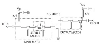
Figure 1 Circuit topology of the Class F power amplifier.
Switching mode PAs, such as Class E, Class F and inverse Class F,2-4 have demonstrated high efficiency, but have the problem of poor linearity caused by the bias at cut-off. To avoid the nonlinear distortions caused by the PAs, DPD is considered one of the most cost effective methods among all the linearization techniques.
In the past few years, many behavioral models have been proposed to characterize the nonlinear and memory effects of the PA.5-7 Among these models, the Volterra series model is considered a general way to model a nonlinear system with memory effects, but it has high computational complexity. The dynamic deviation reduction-based Volterra series model proposed by A. Zhu et al.8,9 and the subsequent simplified vision10,11 not only significantly reduce the complexity of the Volterra series model, but also make the extraction of model parameters more flexible.
This article describes the design of a Class F 2.12 GHz transmitter PA using Cree’s CGH40010 GaN HEMT. The input and output matching networks are designed to optimally approximate the fundamental and second harmonic impedances obtained in source and load pull simulations. The simplified second-order dynamic deviation reduction-based Volterra series model10,11 is used to improve linearity. Both techniques optimize the PA’s intrinsic efficiency-linearity tradeoff. Experimental results with a 20 MHz 4-carrier WCDMA signal and a 20 MHz LTE signal reveal that the digital predistorted Class F PA achieves high efficiency and excellent linearity at an average output power of 33.3 dBm.
Class F Power Amplifier Design
With an infinite number of harmonic terminations, 100 percent drain efficiency is theoretically achievable with square voltage and half-rectified sine current for Class F operation. However, it is not practical in a realistic design to consider an infinite number of harmonic terminations. In this work, only the fundamental and second harmonic impedances are considered. The topology of the circuit is shown in Figure 1.
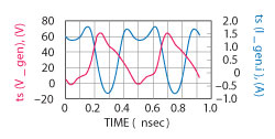
Figure 2 Simulated drain voltage and current waveforms.
The output matching network presents a short at the second harmonic and conjugately matches the transistor’s fundamental output impedance to 50 Ω. The input matching network provides the proper second harmonic impedance at the transistor’s gate to improve efficiency and provides an impedance match with 50 Ω at the fundamental. A resistor connected serially on the input is used to improve circuit stability. To prevent damaging the Class F operation, the λ/4 bias line is placed at the outer side of the network rather than at the drain or gate port of the transistor.
Load Pull/Source Pull Simulation
The Class F PA design is biased with a gate voltage of -2.8 V and a drain voltage of 28 V. The input power level is set to 26 dBm. The load pull/source pull simulation using Cree’s CGH40010 large signal transistor model is carried out with Agilent’s Advanced Design System (ADS) software. The objective is to maximize PAE with a high output power. In this setup, the optimized source and load impedances at the fundamental and second harmonics are determined. The simulation is performed as follows:
- Set the fundamental source impedance at a default value and perform a fundamental load pull simulation to determine the optimum fundamental load impedance (ZL_fund). With a load impedance of ZL_fund, perform a fundamental source pull simulation to obtain the optimum fundamental source impedance (ZS_fund). After several iterations, the optimum fundamental impedances are found to be ZS_fund of (9.1-j1) Ω and ZL_fund of (12.5+j15.8) Ω.
- Perform harmonic load pull simulations with ZS_fund and ZL_fund. In this simulation, only the second harmonic is considered and the impedance value is restricted to be purely reactive. The optimum second harmonic load impedance (ZL_2nd) is j120 Ω.
- Perform harmonic source pull simulation. The optimum second harmonic source impedance (ZS_2nd) is -j18.3 Ω.
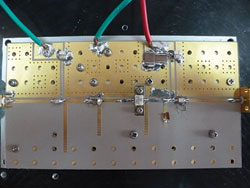
Figure 3 Photograph of the designed Class F power amplifier.
Design of the input and output matching network can be conducted with the optimized impedance values. The design approach has been reported in many experimental works.12,13 Figure 2 shows the simulated drain voltage and current waveforms of the proposed Class F PA. Some distortion of the ideal Class F waveforms may be due to nonlinear parasitics associated with the transistor package. With the optimized source and load impedances, a simulated maximum PAE of 80 percent is predicted at 2.12 GHz with an output power of 40.1 dBm and a transducer power gain of 13 dB.
Implementation and Measurement Results
The Class F PA is fabricated on a Taconic RF-35 substrate with a relative dielectric constant of 3.5 and a thickness of 30 mils (see Figure 3). The gate is biased at –2.8 V, and the drain voltage is 28 V. Figure 4 shows the measured PAE, output power and gain with an input power of 25 dBm from 2.07 to 2.17 GHz. The PAE is greater than 60 percent and output power is greater than 38 dBm from 2.07 to 2.14 GHz. Figure 5 shows the PAE, output power and gain at 2.12 GHz with the input CW signal power level swept from 8 to 28 dBm. A peak PAE of 75.2 percent is achieved with a maximum output power of 39.4 dBm. The actual efficiency may deviate significantly from its theoretical maximum due to device characteristics, bias points, matching network complexity, as well as device and packaging parasitics.
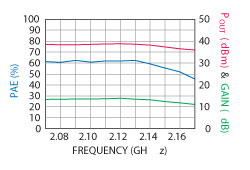
Figure 4 Measured PAE, Gain and Pout versus input frequency with an input power of 25 dBm.
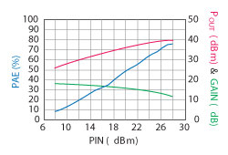
Figure 5 Measured PAE, Gain and Pout versus input power at 2.12 GHz.
Digital Predistortion Experimental Results
The DPD model employed is a simplified version derived from the second-order truncated dynamic deviation reduction-based Volterra model,9 which can be written as:10
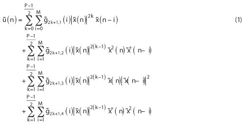
where u~(n) and x~(n) are the complex envelopes of the input and output of the PA, respectively, and g~2k+1,i(.) is the complex Volterra kernel. The symbol (.)* represents the complex conjugate operation and |.| is the magnitude. P and M are the nonlinear order and memory depth, respectively. Only odd-order nonlinearities are considered – i.e., P is an odd number, because the effects from even order kernels can be omitted in a band-limited modulation system.
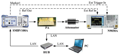
Figure 6 The experimental validation platform for linearization.
The experimental platform4 in Figure 6 is used to validate the linearity improvement of the designed Class F PA. It consists of a vector signal generator (Rohde & Schwarz SMBV100A), a vector signal analyzer (Agilent N9030A), a PC with Matlab and Agilent’s 89600 vector signal analyzer (VSA) software, and the fabricated Class F PA. All the instruments and the PC are connected to a local area network (LAN). The excitation signal can be downloaded from the PC (MATLAB®) to the vector signal generator and the data collected in the vector signal analyzer can be transferred to the PC through the LAN.
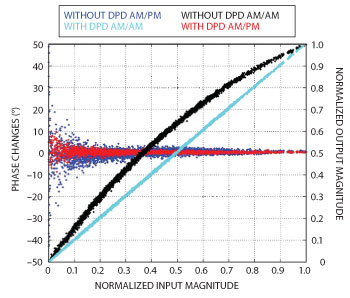
Figure 7 AM-AM and AM-PM plots for the Class F power amplifier with and without DPD.
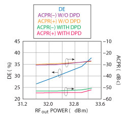
Figure 8 Measured drain efficiency and ACPR versus average output power level with and without DPD.
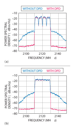
Figure 9 Measured PSD of the power amplifier output with and without DPD for a 20 MHz 4-carrier WCDMA signal (a). Measured PSD of the PA output with and without DPD for a 20 MHz LTE signal (b).
The PA operating at 2.12 GHz is excited by a 4-carrier WCDMA signal with 7.1 dB PAPR. A total of 3556 I/Q samples with an oversampling factor of 4 are generated in MATLAB and downloaded to the vector signal generator. The 20 MHz WCDMA signal is generated by configuring the vector signal generator with a sample rate of 80 Msps. The excitation signal is modulated and up-converted to 2.12 GHz in the SMBV100A, and then distorted by the PA. After appropriate attenuation, the output distorted signal from the PA is down-converted and demodulated by the N9030A. A total of 7112 I/Q samples are captured with a sample rate of 80 Msps. After time alignment and normalization, 3556 samples are used for the PA modeling.
In order to accurately model the nonlinearity and memory effects, the nonlinearity order in the Volterra model is set to 9, while the memory depth is set to 7. The AM/AM and AM/PM plots of the PA with and without DPD are shown in Figure 7. You can see that both nonlinear distortion and memory effects have been successfully compensated. Comparison of the experimental results with the different average output powers are shown in Figure 8. Excellent linearization results in terms of ACPR below –50 dBc are obtained after DPD at the average output power of no higher than 33.3 dBm.
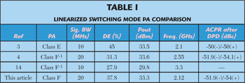
Figure 9(a) shows the measured power spectral density (PSD) of the PA for the WCDMA excitation signal with and without DPD at an average output power of 33.3 dBm. Measured ACPRs are improved to –51.9 dBc (lower) and –54.0 dBc (upper) from –28.3 dBc (lower) and –27.5 dBc (upper), respectively. Figure 9(b) shows the PSD of the PA for the 20 MHz LTE excitation signal at the same output power. ACPR is suppressed to below -53 dBc after DPD. A drain efficiency (DE) of 37.8 percent is achieved. In Table 1, the linearized Class F PA described in this article is compared with a selection of other state-of-the-art linearized switching mode PAs.
Conclusion
A Class F power amplifier using Cree’s CGH40010 GaN HEMT for a 2.12 GHz transmitter application is described. The input and output matching networks are designed to approximate the optimum fundamental and second harmonic impedances obtained through source and load pull simulations. The PA demonstrates 75.2 percent peak PAE with a maximum output power of 39.4 dBm. For the 20 MHz 4-carrier WCDMA signal, the ACPR is suppressed to –51.9 and –54 dBc by using DPD techniques. For the 20 MHz LTE signal, the ACPR is improved to below –53 dBc after DPD. A DE of 37.8 percent is achieved at an average output power of 33.3 dBm.
Acknowledgment
This work is supported in part by the National Natural Science Foundation of China under Grant 60702163, in part by the National Science and Technology Major Project of China under Grant 2010ZX03007-002-01, and 2011ZX03004-003.
References
- F.H. Raab, P. Asbeck, S. Cripps, P.B. Kenington, Z.B. Popovic, N. Pothecary, J.F Sevic and N.O. Sokal, “Power Amplifiers and Transmitters for RF and Microwave,” IEEE Transactions on Microwave Theory and Techniques, Vol. 50, Issue 3, August 2002, pp. 814-826.
- D. Schmelzer and S.I. Long, “A GaN HEMT Class F Amplifier at 2 GHz With >80 Percent PAE,” IEEE Journal of Solid-State Circuits, Vol. 42, Issue 10, September 2007, pp. 2130-2136.
- N. Ui and S. Sano, “A 45 percent Drain Efficiency, -50 dBc ACLR GaN HEMT Class E Amplifier with DPD for W-CDMA Base Station,” IEEE MTTS International Microwave Symposium Digest, June 2006, pp. 718-721.
- J. Wang, Y. Xu and X. Zhu, “Digital Predistorted Inverse Class-F GaN PA With Novel PAPR Reduction Technique,” IEEE International Microwave Symposium Digest, June 2011, pp. 1-4.
- H. Ku and J.S. Kenney, “Behavioral Modeling of Nonlinear RF Power Amplifiers Considering Memory Effects,” IEEE Transactions on Microwave Theory and Techniques, Vol. 51, Issue 12, December 2003, pp. 2495-2504.
- L. Ding, G.T. Zhou, D.R. Morgan, Z. Ma, J.S. Kenney, J. Kim and C.R. Giardina, “A Robust Digital Baseband Predistorter Constructed Using Memory Polynomials,” IEEE Transactions on Communications, Vol. 52, Issue 1, January 2004, pp. 159-165.
- D.R. Morgan, Z. Ma, J. Kim, M.G. Zierdt and J. Pastalan, “A Generalized Memory Polynomial Model for Digital Predistortion of RF Power Amplifiers,” IEEE Transactions on Signal Processing, Vol. 54, Issue 10, October 2006, pp. 3852-3860.
- A. Zhu, J.C. Pedro and T.J. Brazil, “Dynamic Deviation Reduction-Based Volterra Behavioral Modeling of RF Power Amplifiers,” IEEE Transactions on Microwave Theory and Techniques, Vol. 54, Issue 12, December 2006.
- A. Zhu, P.J. Draxler, J.J. Yan, T.J. Brazil, D.F. Kimball and P.M. Asbeck, “Open-Loop Digital Predistorter for RF Power Amplifiers Using Dynamic Deviation Reduction-Based Volterra Series,” IEEE Transactions on Microwave Theory and Techniques, Vol. 56, Issue 7, July 2008, pp. 1524-1534.
- L. Guan and A. Zhu, “Simplified Dynamic Deviation Reduction-Based Volterra Model for Doherty Power Amplifiers,” Workshop on Integrated Nonlinear Microwave and Millimetre-Wave Circuits (INMMIC), April 2011, pp. 1-4.
- L. Guan and A. Zhu, “Dual-Loop Model Extraction for Digital Predistortion of Wideband RF Power Amplifiers,” IEEE Microwave and Wireless Components Letters, Vol. 21, Issue 9, pp. 501-503.
- Y. Xu, J. Wang and X. Zhu, “Analytical Design of an Inverse Class F Power Amplifier for Linear Amplification,” Microwave Journal, Vol. 54, Issue 5, May 2011, p. 146.
- D.Y.T. Wu and S. Boumaiza, “10 W GaN Inverse Class F PA With Input/Output Harmonic Termination for High Efficiency WiMAX Transmitter,” IEEE 10th Annual Wireless and Microwave Technology Conference, April 2009, pp. 1-4.
- D.Y.T. Wu, D. Frebrowski and S. Boumaiza, “First-Pass Design of High Efficiency Power Amplifiers Using Accurate Large Signal Models,” IEEE 11th Annual Wireless and Microwave Technology Conference, April 2010, pp. 1-4