
Modern digital radio transmitter design poses increasing challenges for equipment designers. The ongoing trend towards increased throughput of data is increasing the modulation density and carrier bandwidths of transmitted signals. Peak-to-average ratios increase with higher order modulation schemes and to maintain good adjacent channel power ratio (ACPR) while transmitting the same rms power level, components with lower intermodulation distortion and lower noise must be used.
Baseband, IF and RF bandwidth must be flat across the channel to maintain the spectral shape of the modulated carrier. Furthermore, if digital pre-distortion techniques are being used then the higher order harmonics need to be passed through the baseband inputs and gain flatness must be maintained up to the higher order harmonics of the baseband signal. When a radio transmitter design calls for operation over a very wide range of RF frequencies the RF gain flatness of the overall signal chain becomes critical. Minimizing gain variations in the signal chain over frequency eases the burden of signal chain planning and budgeting. This article focuses on I/Q modulators, which are a critical component in modern transmitters.
A Broadband I/Q Modulator
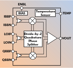
I/Q modulators perform the frequency translation that mixes the baseband signal to the desired location in the RF spectrum. An I/Q modulator consists of a local oscillator (LO) input that is split into in-phase (I) and quadrature (Q) components that are separated by 90°. These two signals drive separate mixers that are also driven by I and Q baseband signals. The outputs from both mixers are then summed to provide a modulated carrier either at RF or IF. The ADL5385 contains these basic blocks (see Figure 1) and is able to achieve a wide tuning range that spans five octaves (50 MHz to 2.2 GHz) through the use of an active divide-by-two LO splitter instead of the more traditional passive polyphase filter. Its wideband performance can be seen in
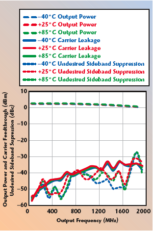
Figure 2, where the output power has a very flat response over the entire output frequency range, with a 1 dB bandwidth of 1300 MHz. This new modulator is designed to directly drive a 50 Ω load and also includes an integrated temperature sensor.
Gauging Signal Quality Using Error Vector Magnitude
Error vector magnitude (EVM) is a measure of the quality of modulation of a signal and it is directly affected by the quadrature and amplitude errors within the modulator. The amount of quadrature and amplitude errors can be gauged by observing the level of sideband suppression in a single-sideband spectrum. Figure 2 shows that the native uncompensated sideband suppression of the ADL5385 I/Q modulator is better than –38 dBc out to 900 MHz. This level of sideband suppression typically yields EVM performance that is more than acceptable for most communication standards. If higher performance is required, sideband suppression can be optimized by adjusting the relative gain and phase of the baseband signals.
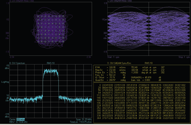
The 64QAM constellation, eye-diagram and spectrum, shown in Figure 3, was generated using random data at 5.056941 MSym/s with a filter alpha of 0.18. This closely mimics the data rate and modulation for a typical cable modem head end application. It can be seen that the EVM for this signal is 0.33 percent rms with a quadrature error of 0.27° and a gain error of 0.003 dB.
Signal Quality vs. Power Level
Figure 4 shows how ACPR varies with output power for the same 64QAM modulated carrier. The high OIP3 of the ADL5385 I/Q modulator enables it to achieve high output power levels with minimal adjacent channel leakage. This results in less gain required in the subsequent stages of the radio.
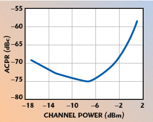
The displayed performance was obtained without digital compensation of the baseband data. This, along with the wide RF tuning range, allows the modulator to be used without factory calibration. This can significantly reduce the time and effort required for design and manufacturing.
Divide-by-two Splitter Enables Broadband Operation
Systems such as cable modem head end equipment must be able to dynamically place carriers anywhere in the the 40 to 900 MHz range. Traditional modulators that use a passive resistor-capacitor polyphase network to split the LO into quadrature components have generally been unable to span such a wide frequency range. This is because the resistor-capacitor networks are tuned for a particular center frequency and typically have a useful range of just over two octaves. Traditional cable modem headend equipment designs use a two-stage up-conversion. The baseband signal is upconverted using an I/Q modulator to an IF frequency above the cable band, typically around 1100 MHz. This IF signal is then mixed down into the cable band using a mixer. These solutions require more components and the complexity associated with such designs increases the design time and effort. System cost and complexity can clearly be reduced if this signal chain could be simplified to a single-stage direct launch architecture.
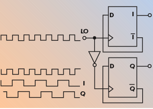
The ADL5385 overcomes the two-octave limitation of traditional I/Q modulators by utilizing a divide-by-two LO splitter. This architecture is illustrated in Figure 5, where two D-flip-flops are clocked by an LO signal and its inversion. In the ADL5385 the inversion is achieved by crossing the polarities of the inputs on one of the differential D-flip-flops. The I and Q signals that drive the mixer cores shown in the ADL5385 block diagram are generated through the alternate clocking of the D-flip-flops by the two LO input signals. Close inspection of the timing diagram on the left of the figure will reveal that it is imperative that the applied LO signal be at twice the desired RF output frequency and that the duty-cycle of that LO signal be exactly 50 percent. Any deviation from 50 percent will degrade the 90° split and this will in turn degrade sideband suppression.
Wide Baseband Bandwidth Increases Data Capacity
In single-channel modulation systems, data capacity can be increased by either using a higher order modulation scheme or by using more bandwidth. Figure 6 shows the normalized baseband frequency response of the ADL5385. With wider carrier bandwidths, the challenge is to maintain a flat gain across the bandwidth of the carrier. This ensures that the spectrum is not distorted by gain ripple. If the gain ripple is too great then precompensation might be required in the digital domain. This process will require the characterization of the frequency response of every radio and will increase the complexity of the design and drive up the cost to manufacture the radio. The ADL5385 offers a 0.1 dB baseband gain flatness out to 85 MHz. This means that for most applications, there should be no need to perform any sort of precompensation.

A Seamless Interface to Baseband I/Q DACs
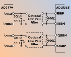
The ADL5385 is designed to interface seamlessly with Analog Devices’ family of transmit digital-to-analog converters (TxDAC). The interface between the two devices typically involves six resistors and a simple LC filter (see Figure 7). The four 50 Ω resistors shunting to ground from each of the DAC outputs provide the 500 mV DC bias for the ADL5385 baseband inputs while the 100 Ω resistor in shunt between each differential pair sets the AC swing of the baseband inputs. With this simple interface the need for single-ended-to-differential or level-shifting amplifiers is eliminated.
Package, Availability, Evaluation Boards
The ADL5385 is packaged in a RoHS-compliant 24-lead LFCSP with exposed paddle. Samples and evaluation boards are currently available and may be ordered on the company’s web site.
Analog Devices Inc.,
Norwood, MA
(781) 329-4700,
www.analog.com.