

Up until a few years ago, it was only possible to fabricate radio frequency power amplifiers (RFPA) in the VHF band by using bipolar transistors, because the devices designed in vertical MOS technology (VMOS), which were the only MOS power devices available at that time, were not able to amplify signals of more than a few hundred megahertz. In fact, the old vertical geometry presents two types of parasitic parameters caused by the transistor layout: the source inductor and the feedback capacitor (gate-drain capacitor), which limit the frequency range to less than approximately 300 MHz. In RF power amplifiers, MOS transistors must be operated in the common-source configuration since the package flange to which the source is electrically connected must be attached to the cooling heat sink (that is the ground), because of thermal problems related to the dissipation of the heat generated. In the same way, BJT transistors are connected in the common-emitter configuration since, in fact, for them the emitter is attached to the flange. For MOS transistors, the common-source configuration (which is analogous to the common emitter of the bipolar transistors) magnifies the capacitance existing between the gate and the drain, because of the Miller effect. In BJT transistors, the capacitance is the one between the base and the collector (see Figure 1). A small value of the capacitance C produces a strong feedback between the output and input, which decreases the gain. From the analysis of their performances, the main difference observed between bipolar and MOS transistors used in RF power applications is the gain: for the same output power level, a BJT has a typical gain value of approximately 8 to 9 dB, while an MOS transistor is able to provide a gain up to 14 dB. From what has been previously demonstrated, if bipolar devices are used as amplifiers between the up-converter and the antenna in the transmission channel, 8 or 9 amplifier stages are necessary. If it is possible to use MOS power transistors, two to three intermediate stages could be eliminated, thanks to their higher gain.
If the number of stages that make up the chain decrease, in addition to the active devices, it is possible to spare the power supply stages, protection circuits and heat sink, and generally decrease cost and size. In this way, it is possible to reduce the probability of failure because the system is made up of a series of several stages: if the number of stages that make up the chain decreases, the reliability will increase because the number of the terms Pi is less (every term is less than or equal to 1), which represents the probability of work for the generic stage.
The unavailability of MOS power devices with high gain and able to work at frequencies in the VHF band has stimulated the research and development departments of the silicon foundries that were already producing RF bipolar transistors to design a new MOS power transistor able to work with good efficiency (over the 300 MHz to 3 GHz frequency range) that is from the UHF to low microwaves (L- and S-bands). The key push for this technological development was caused by the anticipation of a large number of mobile telecommunications sets, first at 900 MHz, then in the dual-band at 1.8 and 2.7 GHz.
Since their introduction in the market, the fields in which LDMOS transistors find application are increasing. The most important one is telecommunications, but many other applications such as military communications and avionics, radar transmitters and broadcasting have been interested by the arrival of the new power semiconductors and benefiting from their optimal performances that represent one important step in digital transmissions.

Technological Development
It was possible to achieve the new LDMOS technology by combining lateral diffusion (LD) with the VMOS transistor (vertical) process in order to avoid the frequency limitations described previously. The reductions of the feedback capacitor and the source inductor have allowed the devices to support high power applications in the frequency range from approximately 300 MHz to 3 GHz. The new LDMOS has been the device of choice in the wireless telecommunications field.
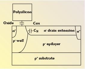
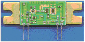
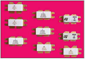
There are two types of technological innovations in the layout of the transistors that have allowed improving the frequency performance of the devices. The first goal has been to reduce the feedback capacitor Cgd, made from the two series capacitors Cox and Csi, where Cox is the overlap capacitor between the gate and the diffused n- drain extension region. It is proportional to the area of such overlap and depends on the oxide thickness. Csi represents the transition capacitor associated with the junction p– well and n– drain extension: this capacitor depends on the depth of the junction and the doping of the n– drain extension region (see Figure 2). The addition of the diffusion region n- drain extension has the effect of reducing the Csi capacitor, which is the larger of the two capacitors in the series, allowing the reduction of the total capacitor Cgd. It is possible to cancel the source inductor by means of the diffusion of one p+ via that forms the contact between the source of the device and its substrate, which has direct contact with the package flange. In such a way, the flange of the device represents the source contact that, in common-source configuration (the only one possible in RF and microwave power applications), must be connected directly to the ground, attaching the same flange of the transistor to the heat sink without electrical insulator, which would make the heat transfer worse. The technological development described, which avoids the use of a bond wire between source and the ground, allows cancelling the associated inductor responsible for the gain decrease that is proportional to the frequency. A cross-section of the LDMOS transistor is shown in Figure 3. An example of the layout of a power amplifier using two LDMOS transistors is shown in Figure 4. It is able to provide approximately 250 W of output power. In the layout, it is possible to observe that the realization of two devices (in push-pull) is made with interdigitated structures in order to optimise the matching. In the layout, it is also possible to observe the impedance matching networks (also called pre-matching networks) that are fundamental for the transformation of the input and output impedances in order to realize the external matching to the standard value of 50 ?. Figure 5 shows some of the LDMOS transistors that are available for use at frequencies up to 1 GHz.
Advantages Compared to the Bipolar Technology
The smaller intermodulation distortion and the better linearity in class A and class AB operations are characteristics that are intrinsic to MOS transistors compared to bipolars, especially if they are used in digital applications. LDMOS transistors have higher efficiency and superior thermal stability, particularly if the bias current for class A is next to the crossing point characteristics. The superior quality of such devices is their gain: its average value is approximately 4 to 5 dB higher than for bipolar transistors for equal output power levels. LDMOS transistors have a typical gain of 13 dB in wideband UHF applications; therefore, they could show gains of over 20 dB in narrowband conditions. It is normal to wait for the LDMOS technology to mature, because it is relatively young and remains subject to reviews and frequent upgrades in order to achieve a better reliability and more resistance to several types of failure. It is important to remember that the new LDMOS transistors, in the same way as the MOS, are intrinsically more delicate than the BJT for accidental electrostatic discharges, which, if induced on the gate, can have deleterious effects (and many times fatal) when they perforate the thin oxide layer present under the same control electrode. Several precautions have been adopted by MOS manufacturers for some time (for example, protection circuits made with diodes have been introduced in the devices in the same package). For the new LDMOS transistors, the most important application is in cell phone base stations. Thanks to the lateral diffusion technology, it is possible to obtain RF power amplifiers able to provide from 5 to 250 W or more output power. These amplifiers require a very good linearity that is necessary to maximize the high data throughput in each channel. The main consideration to achieve that linearity is the DC biasing for optimal drain current for a given power output. Beyond this primary application, the LDMOS technology is finding many other applications in the telecommunications field, where the signal frequencies are extended into the low microwave bands and where the power output levels exceed some hundred watts. LDMOS transistors are used more and more in radar systems, in military communications and in the power amplifiers for TV broadcast. In this last field, only a few years have passed since the advent of these new LDMOS devices. Now, however, every possible co-existence with RF amplifiers using the old bipolar technology has already been excluded.
For broadcast applications, the LDMOS technology has clearly shown advanced characteristics compared to what is possible from equipment using BJT transistors, such as the linearity of the video parameters, and harmonic and intermodulation distortions, the main characteristics for the transformation of the actual transmission video systems to the digital signal systems of digital video broadcasting-terrestrial (DVB-T) type. Only by using amplifiers with LDMOS transistors is it possible to achieve a good minimization of the output power back-off, a representative parameter of the loss of power available due to the conversion of a traditional transmission system to the new standard DVB-T. Only with this innovative technology is it possible to exercise one good pre-correction on the digital signal in the pre-modulation stage. Thanks to this operation, which is very effective only with LDMOS technology, it is possible to contain the output back-off and therefore to have a reduction in the available output power f approximately 3 dB, an output power reduction that becomes approximately 7 dB if the conversion operation is made on equipment using bipolar transistors.