
High efficiency microwave amplifiers with low supply voltages are required for mobile telecommunications services, such as GSM or DCS1800 systems. Theoretically, class-F power amplifiers (PA) can achieve 100 percent drain efficiency by maximally flattening the voltage and current waveforms of the active device.1 By increasing the efficiency of the microwave amplifier, the dissipated power is reduced while the output power is increased. Therefore, a reduction in size and weight of portable wireless transmitters is achieved, as well as prolonged battery life.
Many amplifier modes of operations are available to designers in their quest to improve efficiency, such as class-F,2–4 single-ended class-B,5 push-pull class-B6 and harmonic reaction.7–8 Although they have different theoretical backgrounds, the basic principle involved in increasing their efficiency is the same, that is minimizing the power dissipation across the active devices. Here, the class-F operation is preferred as it offers the possibility of controlling the impedances at a finite number of harmonics.1 It also provides a high efficiency and has a simple circuit construction.9 Though many papers have been published on class-F PAs, a detailed design procedure is still needed to aid in practical construction. The purpose of this article is to present a design procedure for a class-F PA with an example given at 900 MHz.
Design Parameters and Procedure
In low bias voltage operation, the knee voltage in the active device will affect the PAE. Therefore, the knee voltage is one of the design considerations and leads to the selection of a pseudomorphic high electron mobility transistor (PHEMT), since the knee voltage of HEMTs is lower than that of GaAs MESFETs.10 Also, the device manufacturer supplies a large-signal device model for this active device, which allows better initial models to be built. The typically stated small-signal S-parameters and static IV curves are only applicable for small-signal levels and therefore do not provide accurate modeling of the device behavior as a PA.11 A large-signal device model is necessary for the accurate simulation of PAs using the harmonic balance method.
The important design parameters in PAs are power-added efficiency (PAE), drain efficiency (ηd) and power gain (Gp). PAE is defined as the ratio of the additional RF power provided by the amplifier to the DC power:12

where Pin is the RF input power.
PAE can also be rewritten as

where ηd is the drain efficiency defined by

and Gp is the power gain defined by

The amplifier must also be evaluated for its stability condition using large signal S-parameters (LSSP) over a wide band of frequencies. This measurement gives the distance from the center of the Smith chart to the nearest output (load) stability circle. This stability factor is given by13

where Δ is the determinant of the scattering matrix.
If µ > 1, the device is unconditionally stable. This single parameter can replace the dual Rollet (K > 1) and auxiliary conditions for determining unconditional stability. It is noticed that the active device alone is unstable over almost the entire frequency range (low frequency to fmax) due to its high transconductance. Therefore, a stabilizing circuit is required to make sure the circuit is unconditionally stable from low frequency to fmax.
The design starts with DC simulation, when some useful active device RF parameters are obtained, as shown in Table 1. The simulation has been carried out using the Advanced Design System (ADS) software tool.

An extensive large-signal harmonic balance analysis, based on the “Substitute Generator Technique,”14 has been used to optimize the source and load impedance at the fundamental frequency, as well as the load impedances at the third harmonic, required for class-F operation. In this method, two independent generators are used to force the voltage waveforms (magnitude and phase) at the gate and drain ports of the active device, as shown in Figure 1. The phase angles of the drain voltage at the fundamental frequency (θ1) and the third harmonic (θ3) are tuned to obtain the maximum PAE, while the magnitude and phase angle of the drain voltage at the second harmonic are fixed at zero.

Fig. 1 The substitute generator technique.
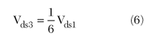
The phase angles of the drain voltage at the fundamental frequency (θ1) and the third harmonic (θ3) are tuned to obtain the maximum PAE, while the magnitude and phase angle of the drain voltage at the second harmonic are fixed at zero. To obtain a near square drain voltage, the magnitude of the drain voltage at the third harmonic should be 1/6 of the magnitude of the drain voltage at the fundamental frequency14
The choice of bias circuit is based on the desired class of operation and power supply requirements of the PA. To fulfill the requirement of a mobile handset, a low drain bias voltage, Vds = 3 V, is applied in this PA circuit. Meanwhile, in class-F operation, the active device is biased in deep class-AB for a quiescent drain current value of 0.15 Idss; the gain problems associated with small signals, therefore, can be partially overcome. In addition, a low quiescent drain current causes a small mean value of Id0 to reduce the dissipation in the active device.15 It is advisable not to bias at class-B because the small-signal and power gain performance of the amplifiers is drastically degraded at or very near pinch-off.5 95 Ω quarter wavelength microstrip lines are used to isolate the DC voltage supplies from the RF signals at the gate and drain. Further RF shorts are achieved using bypass capacitors that can provide suitably low impedances over the desired frequency range. In this case three bypass capacitors have been selected, of value C1 = 27 nF, C2 = 100 pF and C3 = 100 pF, as shown in Figure 2. To satisfy the bypass capacitor application requirements, the series resonant frequency (fSR) and the magnitude of the impedance should be evaluated throughout the desired frequency range.16 Figure 3 shows impedance versus frequency for the three different values of the bypass capacitors (C1, C2, C3) used in this design. From this figure it is seen that the fSR occurs at or close to the desired “bypass frequency;” therefore, the low impedance at fSR makes these capacitors suitable for bypassing applications from a few megahertz up to approximately a gigahertz. The input and output ports are DC blocked by using C4 = 100 pF and C5 = 10 pF series capacitors, respectively.
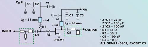
Fig. 2 Circuit diagram of the power amplifier.

Fig. 3 Impedance vs. frequency for three bypass capacitors.
The matching networks are the crucial parts of PAs. An important consideration in designing PAs using packaged FET devices is to accurately determine the package parasitic elements, which affect the load and source impedances. The device’s Cds and all drain and source package parasitic elements must be included as a part of the total output matching circuit.11,17–18 Generally, the input matching circuit transforms the gate impedance of the active device to the 50 Ω source for high power gain, while the output matching circuit transforms the drain impedance of the active device to a 50 Ω load for maximum RF output power. For class-F operation, the output matching network also acts as a tuning circuit for the third harmonic. Therefore, the output matching network becomes an even more challenging task. The output matching circuit has a bandpass topology, which consists of three microstrip lines. The quarter wavelength short-circuited stub at the fundamental frequency, which is a part of the drain bias circuit, presents a low impedance to reflect the second harmonic back into the drain while it has no influence on the fundamental and third harmonic impedances. Due to the package reactance at the drain, the second harmonic load impedance (1.36-j18)Ω has been optimized to improve performance. This gives rise to a 2.5 percent improvement in PAE when compared with a shorted second harmonic load impedance (0.001 Ω). To produce a nearly square wave at the drain, an open-circuited stub and a series microstrip line are used to create the desired high impedance at the third harmonic. The output matching network also includes a 10 pF DC block capacitor (C5). Table 2 shows the load impedances with different harmonic termination at the second and third harmonics. The simulation results show that there is an improvement in PAE of more than 5 percent with the optimum load impedances (This case) in comparison to the one with the short circuit at the second and third harmonics (Case 1), while a 13 percent PAE improvement is obtained when compared with a 50 W load impedance at the second and third harmonics (Case 2).
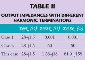
Figure 4 shows the simulated loadline and associated drain voltage/current waveforms. These are obtained using the optimum load impedance condition for the fundamental frequency coupled with output harmonic tuning at the second and third harmonics. Since the overlapping area between voltage and current waveforms is small, it can be deduced that the power dissipation in the active device will be small, while the PAE increases.
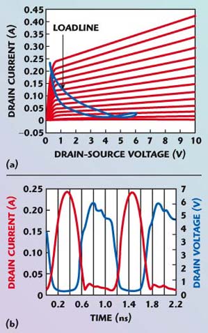
Fig. 4 Simulated loadline (a) and drain current and voltage waveforms (b) required for maximum PAE of a class-F power amplifier.
The device input is matched to 50 Ω via a classical approach, a three-element T-network, consisting of a short-circuited stub and two series microstrip lines. The stabilizing resistors R1 = 33 Ω and R2 = 30 Ω decrease the Q of the network and therefore provide a wider bandwidth of input matching. These matching networks are fabricated using distributed elements to reduce the insertion loss. In general, it is advisable to minimize the number of elements, to reduce power loss, circuit complexity and parts cost.
It is also very important to include all component parasitic elements in the design. Not many component manufacturers provide the exact parasitic value of passive components such as vias, SMT capacitors and SMT resistors, so a fixture is designed to extract their S-parameters using a network analyzer.
To add to the stability, a 33 Ω resistor (R1) is placed in series with a quarter wavelength shorted stub at the gate bias network, while another 30 Ω resistor (R2) is placed near the gate port, as shown in the circuit diagram. This network greatly enhances the PA’s stability, which means the PA circuit becomes stable over the whole frequency range (2 MHz to 10 GHz), as shown in Figure 5. The advantages of this network come at a price; the stabilizing resistors degrade the performance of the circuit at all frequencies, therefore an appropriate amount of minimum loss resistors that lead to a borderline stability where µ reaches 1 are recommended at the input to the active device.19 It is good practice to avoid adding any stabilizing resistors in the output network because the amplifier efficiency will drop drastically with any loss in the output network.

Fig. 5 Stability factor vs. frequency.
Measurement Results
The complete amplifier circuit is constructed on PCB, RT Duroid 5870 with a dielectric constant of 2.33, a thickness = 1.575 mm and tanδ = 0.0012. The bias networks, active device and matching networks are confined within the PCB board (dimension 85 by 50 mm). A photograph of the complete PA module is shown in Figure 6. Three via holes are added at the active device source to provide low inductance to ground. The zener diodes in the drain and gate bias networks are used to provide additional protection against transients, reverse biasing and overvoltage.20
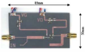
Fig. 6 The fabricated class-F power amplifier operating at 900 MHz.
A measured peak PAE of 71.4 percent with Pout = 22 dBm and Gp = 14 dB (2.3 dB compression) is achieved at a low drain voltage Vds = 3 V and Pin = 8 dBm. The measured PAE, Pout and Gp performances versus Pin and frequency are shown in Figures 7 and 8, respectively. A PAE above 60 percent is achieved over a frequency range of 850 to 970 MHz (13 percent BW).

Fig. 7 Measured PAE, Gp and Pout as a function of Pin.

Fig. 8 Measured PAE, Gp and Pout as a function of frequency for Pin = 7.5 dBm.
Conclusion
The design methodology and selection criterion for a high efficiency PA operating in the GSM band is presented in this article. A PAE of more than 71 percent with Pout = 22 dBm and Gp = 14 dB has been obtained at a very low drain voltage of 3 V. From the measurement results, it can be concluded that efficient PAs can be obtained through the appropriate choice of active device, operation mode and optimum load impedance terminations at the fundamental frequency, second and third harmonics. Practical design considerations such as device (active and passive) and package parasitic elements also must be taken into account. This PA module shows its potential for use in mobile communication devices since it is able to achieve a high efficiency at a very low drain voltage.
Acknowledgment
This project is funded by EPSRC, UK, under grant no. GR/S42538/01. Donation of the Advanced Design Systems (ADS) software tool from Agilent Technologies is also acknowledged.
References
- F.H. Raab, “Class-F Power Amplifiers with Maximally Flat Waveforms,” IEEE Transactions on Microwave Theory and Techniques, Vol. 45, No. 11, November 1997, pp. 2007–2012.
- C. Duvanaud, S. Dietsche, G. Pataut and J. Obregon, “High Efficient Class-F GaAs FET Amplifiers Operating with Very Low Bias Voltages for Use in Mobile Telephones at 1.75 GHz,” IEEE Microwave and Guided Wave Letters, Vol. 3, No. 8, August 1993, pp. 268–270.
- J.C. Pedro, L.R. Gomes and N.B. Carvalho, “Design Techniques for Highly Efficient Class-F Amplifiers Driven by Low Voltage Supplies,” IEEE International Conference on Electronics, Circuits and Systems, Vol. 3, September 1998, pp. 201–204.
- K. Chiba and N. Kanmuri, “GaAs FET Power Amplifier Module with High Efficiency,” Electronics Letters, Vol. 19, No. 24, November 1983, pp. 1025–1026.
- J.R. Lane, R.G. Freitag, H.K. Hahn, J.E. Degenford and M. Cohn, “High Efficiency 1-, 2- and 4-W Class-B FET Power Amplifiers,” IEEE Transactions on Microwave Theory and Techniques, Vol. 34, No. 12, December 1986, pp. 1318–1326.
- S. Toyoda, “High Efficiency Single and Push-pull Power Amplifiers,” IEEE MTT-S International Microwave Symposium Digest, Vol. 1, June 1993, pp. 277–280.
- T. Nojima, S. Nishiki and K. Chiba, “High Efficiency Quasimicrowave GaAs FET Power Amplifier,” Electronics Letters, Vol. 23, No. 10, May 1987, pp. 512–513.
- S. Nishiki and T. Nojima, “Harmonic Reaction Amplifier – A Novel High Efficiency and High Power Microwave Amplifier,” IEEE MTT-S International Microwave Symposium Digest, Vol. 2, June 1987, pp. 963–966.
- T.L. Lin, T.H. Liu and Y.H. Kao, “Fabrication of High Efficiency Power Amplifier Module for Cellular Mobile Phone,” Proceedings of National Science Council, ROC (A), Physical Science and Engineering, Vol. 20, No. 6, November 1996, pp. 651–659.
- Y. Takayama, “Considerations for High Efficiency Operation of Microwave Transistor Power Amplifiers,” IEICE Transactions on Electronics, Vol. E80-C, No. 6, June 1997, pp. 726–733.
- A. Sweet, “MESFET Power Amplifier Design: Small Signal Approach,” Design Seminar, Agilent Technologies, 2001.
- S.A. Maas, Nonlinear Microwave and RF Circuits, Artech House Inc., Norwood, MA, 2003.
- M.L. Edwards and J.H. Sinsky, “A New Criterion for Linear Two-port Stability Using a Single Geometrically Derived Parameter,” IEEE Transactions on Microwave Theory and Techniques, Vol. 40, No. 12, December 1992, pp. 2303–2311.
- A. Mallet, T. Peyretaillade, R. Sommet, D. Floriot, S. Delage, J.M. Nebus and J. Obregon, “A Design Method for High Efficiency Class-F HBT Amplifiers,” IEEE MTT-S International Microwave Symposium Digest, Vol. 2, June 1996, pp. 855–858.
- J. Huang and D. Zhan, “High Efficiency FET Power Amplifier with Very Low Drain Bias for Mobile Communication,” IEEE MTT International Topical Symposium on Technologies for Wireless Applications, 1995, pp. 123–126.
- R. Fiore, Circuit Designer’s Notebook: Capacitors in Bypass Applications, American Technical Ceramics.
- J.L.B. Walker, High Power GaAs FET Amplifiers, Artech House Inc., Norwood, MA, 1993.
- S.C. Cripps, RF Power Amplifiers for Wireless Communications, Artech House Inc., Norwood, MA, 1999.
- R. Gilmore and L. Besser, Practical RF Circuit Design for Modern Wireless Systems: Active Circuits and Systems (Volume 2), Artech House Inc., Norwood, MA, 2003.
- G. Gonzalez, Microwave Transistor Amplifiers: Analysis and Design, Second Edition, Prentice-Hall Inc., Upper Saddle River, NJ, 1996.