Radio frequency micro-structured inductors are currently being developed to optimize the transmission and filtering features for microwave applications like RFIDs, radars, satellite communications and medical sensors. This technology is also of interest for the next generation wireless communication devices and biomedical instruments. To fulfill these requirements, different design techniques have been developed for the miniaturization of inductors.1-3 This article proposes a new method for the design and fabrication of high quality factor micro-solenoids.
On-chip inductors such as micro-spirals,4-6 micro-solenoids7-10 and micro-toroidals,11 have been extensively studied. Among the circuit parameters related to micro-inductors is the parasitic capacitance between the coil and the ground, which has a significant effect on the resonance frequency and the quality factor of the actual inductor. For example, on-chip micro-spirals have large parasitic capacitance between the coil and the substrate. However, several design techniques, including ground shielding, suspended micro-coils and isolation layers, have been developed to decrease this capacitance. Nevertheless, the on-chip micro-spirals are not able to provide Q-factors greater than 100.12-14 Alternatively, to overcome the parasitic capacitance, different on-chip micro-solenoid structure schemes have been made but they require complex fabrication. For example, to make a suspended micro-solenoid with low parasitic capacitance, one needs five layers of photolithographic patterning. Regardless of the improvements in their Q, these coils are currently unreliable as commercial devices.15
A few approaches have been proposed to enhance quality factor by the making of off-chip micro-inductors. New substrates were used for the sake of lower parasitic capacitance. Soh et al. used a high resistivity silicon wafer to build the micro-solenoid using vias through the wafer.16 Nevertheless, this method had an uncommon process and did not offer Q-factors higher than 18.5. Yoon et al. and Lu et al. have used Pyrex glass as the substrate, which decreased the capacitive coupling and substrate loss in the fabrication of micro-solenoids.17,18 However, the resulting quality factor was still less than 100. Other approaches were the application of alumina as a microwave substrate, system on package (SoP) using LTCC and organic packaging substrates for making spiral and helical RF inductors. These techniques can provide Q-factors higher than 100, but they all suffer from multi-layer and costly fabrication process.19-21
In a recent study, a microwave substrate material with a low relative dielectric constant of 2.2 was used for making micro-toroidals, using microstrip or stripline.22 This research showed an improvement of 1.5 times, when compared to the conventional micro-spiral inductors. Due to the microstrip grounding layer in the middle of the toroidal, the maximum Q was obtained for frequencies less than 1.25 GHz and the thickness of the actual multi-layer dielectric board became more than 3 mm. They have shown quality factors higher than on-chip inductors, but the application of monolithic commercial microwave printed circuit boards (PCB) production method with common thicknesses for micro-electronic structures has not been investigated in the literature. Standard PCB techniques decrease the cost and complexity of the devices, when compared to the other micro-inductor counterparts.
The use of microwave PCBs as a dielectric substrate for micro-inductors is not only an important factor for the commercialization and ease of fabrication, but it also benefits from a variety of different relative dielectric permittivity and substrate thicknesses available in PCB materials. The permittivity is a major parameter to decrease the loss in the substrate and optimize the quality factor. The current study, which is a preliminary research,23 was done to find a commercial monolithic design and a creation method for micro-solenoids with low parasitic capacitance, using common microwave PCBs.
This article describes the design, fabrication and test of novel off-chip solenoid inductors for RF frequency applications. The inductor consists of a micro-solenoid embedded inside a RT/Duroid 5880 circuit board. The low relative permeability of 2.2 helps to keep a low stray capacitance as well as low loss for the fields inside it.24,25 Due to the difficulty of drilling high aspect ratio vias close to each other, this effort was limited to a drilling diameter of 0.250 mm in order to achieve the maximum possible resonance frequency. Various lengths, heights and pitch sizes were modeled to find the best response. A set of the resulting devices, with different size parameters based on our modeling, were used to optimize the experimental resonant frequency and quality factor.

Figure 1 Diagram of a two-turn solenoid on a Duroid substrate.
A schematic diagram of the solenoid is shown in Figure 1. Each solenoid consists of at least ¾ of a turn patterned through the printed circuit board and two electrical feed lines of length a/2. Thus, for this design, the first turn of the solenoid begins at the start of the diagonal beam section patterned on top of the substrate. Each diagonal section represents an additional turn in the device. This allows the user to quickly identify the number of turns present in the structure by counting the number of diagonal lines patterned on the top surface of the substrate. Using this design rule, the solenoid has two diagonal beam sections and is, therefore, a two-turn device.
Two modeling techniques were used to investigate the circuit. The analytic modeling of the circuit was done using a single π-circuit model. An electromagnetic simulation of the device was also done with Ansoft-HFSS software. The simulated results were compared to the measured S-parameters of the fabricated devices, using a microwave probe station. Both the inductance and quality factor were evaluated. The experimental data shows close agreement between modeling and simulation. The low cost standard PCB production technique decreased the cost and complexity of device commercialization, when compared to micro-inductors counterparts.
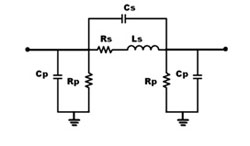
Figure 2 π-model schematic for a micro-selenoid inductor.
Theory
A single p-circuit model was used to describe the micro-solenoid. It can be used for solenoids with a considerable distance from the shielding.26 Using the Greenhouse-Grover method, the self inductance of each segment as well as the mutual inductance between them27 was determined. The capacitive behavior of this device includes the two different capacitances, which are Cs, the stray capacitance between segments, and Cp between segments and ground. Based on the position of the segments, the capacitances are in air or inside the Duroid substrate with a dielectric constant of 2.2. All segments and the capacitances between them have been considered in the following model. The resulting π-circuit is illustrated in Figure 2 and the parameters of the circuit are evaluated as follows:
Inductances
The fabrication of the coil requires the use of both rectangular and cylindrical components. Each geometric condition must be solved in order to find the inductance of the complete coil. The self inductance of a circular via inside the substrate is named Lcs, with the approximate value of:27

Likewise, the self inductance of each rectangular segment can be approximately evaluated by, Lrs in nano-Henries:

where l is the length, h is the height (and substrate thickness), b is the thickness and w is the width of the conductor. It should be noted that the beam rectangular segment length, l, has two values in this design. And, thus, there are two rectangular inductance values, one for l = a, and another for

The leads connecting the coil to the RF contact pads have a length of a/2.
The mutual inductance M, between each couple of segments, can be evaluated by:27 M = 2lG
It is positive if the current in both segments is in the same direction and negative if it is in opposite direction. To find the G, the following relations can be used:

where D is the geometric mean-distance relating the width and pitch of the line segments as defined by Greenhouse:27

The total inductance is the sum of all self inductances and mutual inductances in a turn coil. Recalling that each n turn coil actually consist of n + ¾ turns, then the total inductance is the sum of the inductance due to n loops plus a three quarter turn loop with a rectangular beam length, l = a as follows:
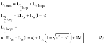
The values of the mutual inductances are reduced by the distance between segments, so the major mutual inductances occur between top and bottom conductors. This helps to approximate the mutual and self inductances of one turn and simplify the formula due to the reoccurrence of the turns.
Capacitances
As previously stated, the single π-circuit model uses two capacitive elements, stray and parallel. The stray capacitances are between the segments from the first terminal to the second. These depend on the cross-section, distance, and the dielectric constant between segments.
Despite the fact that the capacitances between via are much higher than the other segments, the calculation of stray capacitance, Cs for an n turn solenoid of pitch, d, of individual line segments, relies on the capacitance between all adjacent segments and is formulated as follows:
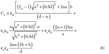
Each segment also demonstrates a capacitance to the ground, as stated by the parallel capacitive features, Cp, of the two-port network. This parasitic term consisted of the capacitances of lower segments to the ground, CL, and capacitances of upper segment to ground, CU. A few added dimensional constraints are required to adequately evaluate these capacitances. First, the distance between the line metal line segments on the bottom of the substrate and ground, lb, is tailored to reduce these terms in the system. The width of the gap between the coil and the ground pads is approximately 25 µm (the thickness, b, of the rectangular section). Finally, the closest distance between the coil turns and the ground loop is approximately one half of the metallic lead width, w.

Resistances
The series resistance includes the resistances of surface conductors in series with the resistances of the columns. The skin effect should also be considered for this calculation.
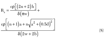
where c represents the resistivity ratio of the bulk metal to that of the electroplated metal. For simplicity, c was set to a value of one in this experiment.7 Also ρ is the resistivity of copper, δ is the skin depth and is given by:28

In which µ is the permeability of copper and f is the frequency of the electromagnetic field.
After developing terms for the individual circuit components, the π-model was then solved for in terms of a one-port measurement to match the experimental requirements for testing. In a one-port measurement, the second terminal of circuit model is connected to ground and the equivalent π-model of the circuit results in the following quality factor:13

Design and Fabrication
Based on the equation provided for the modeling, one can design a specific coil to match the Q factor desired in the range between 2 and 6 GHz. To achieve the highest resolution, this project is focused on the use of RT/Duroid 5880, with the very low relative permittivity of 2.2. This benefits low loss through the entire thickness of the board. Three-dimensional structures in RF substrates have multiple different applications, including high quality factor resonators, microstrip antennas and interconnects.25,29 As such, the key to this design is to pattern the micro-solenoid through the Duroid to maintain a uniform magnetic field through the coil. This is achieved through the utilization of a small diameter coil comprised of a low resistivity metal that does not oxidize on the surface. While gold is ideal for such cases, copper is cheaper and, therefore, easier to demonstrate in a laboratory experiment.
In order to maintain the compatibility of standard printed circuit board process, the drilling size of 125 µm radius was used. To match this requirement, the width of each conductor would be 250 µm and the minimum distance between two conductors was 250 µm. Copper or silver can be used as the cladding layers. Here, copper cladding with silver immersion layer technology was used for the surfaces. A thin finishing layer of gold is added to avoid the oxide growth. Each via was electroplated simultaneously to make the columns. In the two-turn inductor depicted previously, h is the height of the vias, w is the width of the surface conductors, a is the bottom layer conductor length, d is the pitch size and b is the thickness of the cladding layer. The following variables were used to maximize the quality factor:
- Substrate thickness (h)
- Pitch size (b)
- Surface conductor length (a)
- Number of turns (n)
- Wire width (w)
To realize the effect of columns height on the design, two Duroid thicknesses of 3.0 and 0.380 mm were provided. In order to determine the maximum value for Q for each substrate thickness, 16 different sizes of solenoid have been designed, simulated, fabricated and tested. The original space included four different coil designs. Each design was studied for four different numbers of turns.
The one-port quality factor, Q11(ω), is considered a measure for the performance of the coils in most literatures.5 It has been defined as:

The Y11 can be calculated in port one, while the second port is short circuited. The inductance L is equal to:


Figure 3 Q factor and inductance as a function of the number of turns.
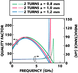
Figure 4 Q factor and inductance as a function of a.
Figure 3 shows the Q-factor and inductance as a function of the number of turns, with a = 1 mm, d = 0.5 mm, h = 0.38 mm and w = 0.25 mm, using the electromagnetic simulation by Ansoft HFSS. Figure 4 illustrates the influence of the top conductor length, a, on the Q-factor. Figure 5 shows the result of change in the pitch size, d. Increasing the substrate thickness or height will increase the inductance, but the quality factor will decrease. Optimization of the results using the analytical modeling and electromagnetic simulation showed that a one-turn solenoid, with 0.380 mm columns height and 1 mm of the surface conductor length also 0.250 mm pitch, can provide the maximum Q factor of 160.3. A copper conductivity of
4 × 10⁷ S/m was used to match the simulation with the conductivity of our electroplated copper. A photograph of the micro-solenoids is shown in Figure 6.
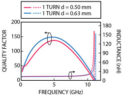
Figure 5 Q factor and inductance as a function of d.

Figure 6 Top view of the micro-solenoids in their ground pad for a = 1 mm, w = 0.250 mm and d = 0.500 mm.
Results and Discussion
The S-parameters of the fabricated resonators were measured using a HP8363 network analyzer and GSG Cascade Microtech probes. The short-open-load-thru (SOLT) calibration has been done with an impedance standard substrate (ISS). The frequency span was measured using 6800 sampling points to increase the accuracy. Samples were put on a striped Duroid board of 3.0 mm thick to decrease the ground capacitance during measurement. De-embedding of the pads was carried out after conversion of S-parameters to Y-parameters. The Y-parameters of an open pad was subtracted from the same measured one for a solenoid in the pad. Then the S-parameters were calculated using the new Y-parameters.30 The Q-factors and inductances were evaluated using the equations shown previously.

Figure 7 Measured Q and inductances of a micro-solenoid as a function of the number of turns.
The results of the measurement for one, two and three turns inductors of model-1, including a = 1 mm, d 0.5 mm, h = 0.38 mm and w = 0.25 mm, are illustrated in Figure 7. The circuit parameters of this model for substrate thicknesses of 0.380 and 3.010 mm are given in Table 1.

The resulting measurements showed that the application of low relative permittivity material like RT/Duroid 5880 did not degrade the quality factor due to the low dielectric permittivity. Furthermore, the Duroid was a good supporting substrate to fabricate a reliable solenoid structure. Optimization of the quality factor in the micro-solenoid resulted in closely spaced conductors to provide the highest coupling of the magnetic field. Besides that, the conductors should be wide enough to reduce the resistivity of the overall inductor. To show the compatibility of the measurement with the analytical modeling and EM-simulation all three results for the one-turn inductor are compared in Figure 8. In this model, a quality factor of 160.3 has been measured for a one-turn solenoid with 0.380 mm column height and 1 mm of the surface conductor length and a 0.250 mm pitch size.

Figure 8 Comparison between simulated and measured Q factors of a single turn micro-solenoid inductor.
The major restriction for increasing the quality factor in this inductor was the resistivity of the electroplated copper, which was higher than the bulk copper. The increased resistance observed in the electroplated material lowered the measured Q-factor. As such, Figure 9 shows that, for an inductor of 3.01 mm thickness, with a = 1 mm, w = 0.250 mm, h = 0.380 mm and d = 0.500 mm, the Q did not match the modeling results, due to higher resistivity of the actual fabricated device. Any improvement in the metal via fill process can result in a future enhancement of the quality factor for micro-solenoids.

Figure 9 Q factor of a 3.01 mm thick substrate micro-solenoid with a single turn.
If a resistivity close to that of the bulk metal could be achieved in the electroplated vias, then quality factors higher than 200 could be obtained. For example, if this research compared to the micro-spirals on the alumina substrate and micro-coils using SoP structures, it not only benefits from higher quality factor but also has a commercial production method that can be realized.20,21 In contrast to the toroidal inductors reported by Philips and Settaluri with microstrip or stripline, the current results show that the monolithic structures decrease the capacitive effects of close grounding layer and increase the self resonance frequency of inductors.23 Power management is also higher due to the increased cross-section for the conductors.31 Finally, the device presented in this work benefits from a commercial thickness for the board, higher frequency for the maximum Q, and easier monolithic fabrication. These advantages make the resulting micro-solenoid a good candidate for the miniaturization of the commercial off-chip inductors.
Conclusion
Design, simulation and fabrication of novel off-chip micro-solenoids with high quality factor are reported. Low cost standard PCB fabrication was used. The S-parameters of the fabricated models were measured using a microwave probe station and the quality factor has been extracted. A maximum quality factor of 160 was recorded for a one-turn solenoid. It shows close agreement with modeling. The results have a potential application in microwave circuits to enhance their performance with keeping a very high quality factor. It would also decrease the cost, and complexity of fabrication compared to on-chip resonators, and MEMS structures.
Acknowledgment
The research presented above was supported by the Alabama EPSCoR GRSP program. Special thanks to Chris Nordquist at Sandia National Laboratories.
References
- S.K. Kuo, S.L. Chen and C.T. Lin, "Design and Development of RFID Label for Steel Coil," IEEE Transactions on Industrial Electronics, Vol. 57, No. 6, June 2010, pp. 2180-2186.
- D.E. Mouzakis, D. Dimogianopoulos and D. Giannikas, "Contact-Free Magnetoelastic Smart Microsensors With Stochastic Noise Filtering for Diagnosing Orthopedic Implant Failures," IEEE Transactions on Industrial Electronics, Vol. 56, No. 4, April 2009, pp. 1092-1100.
- D.F. McCann, M. Wark, P. Millard, D. Neivandt and J.F. Vetelino, "The Detection of Chemical and Biological Analytes Using a Monolithic Spiral Coil Acoustic Transduction Sensor," 2008 IEEE Ultrasonics Symposium Digest, pp. 1187-1190.
- W. Xu, S. Sinha, T. Dastagir, W. Hao, B. Bakkaloglu, D.S. Gardner, C. Yu and Y. Hongbin, "Performance Enhancement of On-Chip Inductors With Permalloy Magnetic Rings," IEEE Electron Device Letters, Vol. 32, No. 1, January 2011, pp. 69-71.
- C.H. Ahn and M.G. Allen, "Micromachined Planar Inductors on Silicon Wafers for MEMS Applications," IEEE Transactions on Industrial Electronics, Vol. 45, No. 6 , December 1998, pp. 866-876.
- A.M. Niknejad and R.G. Meyer, "Analysis, Design and Optimization of Spiral Inductors and Transformers for Si RFICs," IEEE Journal of Solid-state Circuits, Vol. 33, No. 10, October 1998, pp. 1470-1481.
- C.M. Tai and C.N. Liao, "A Physical Model of Solenoid Inductors on Silicon Substrates," IEEE Transactions on Microwave Theory and Techniques, Vol. 55, No. 12, December 2007, pp. 2579-2585.
- L. Gu and X. Li, "High-Q Solenoid Inductors with a CMOS-compatible Concave-suspending MEMS Process," IEEE Journal of Electromechanical Systems, Vol. 16, No. 5, October 2007, pp. 1162-1172.
- J.M. Yook, J.H. Ko, M.L. Ha and Y.S. Kwon, "High-quality Solenoid Inductor Using Dielectric Film for Multichip Modules," IEEE Transactions on Microwave Theory and Techniques, Vol. 53, No. 6, June 2005, pp. 2230-2234.
- S. Waselikowski, K. Kratt, V. Badilita, U. Wallrabe, J.G. Ulrike and M. Walther, "Three-dimensional Microcoils as Terahertz Metamaterial with Electric and Magnetic Response," Applied Physics Letters, Vol. 97, No. 26, December 2010, pp. 261105-261105-3.
- V. Ermolov, T. Lindstrom, H. Nieminen, M. Olsson, M. Read, T. Ryhanen, S. Silanto and S. Uhrberg, "Microreplicated RF Toroidal Inductor," IEEE Transactions on Microwave Theory and Techniques, Vol. 52, No. 1, January 2004, pp. 29-37.
- C.P. Yue and S.S. Wong, "On-chip Spiral Inductors with Patterned Ground Shields for Si-based RFIC's," IEEE Journal of Solid-state Circuits, Vol. 33, No. 5, May 1998, pp. 743-752.
- Z. Jun, W. Changhai and A.J. Sangster, "Theoretical and Experimental Studies of Flip-chip Assembled High-Q Suspended MEMS Inductors," IEEE Transactions on Microwave Theory and Techniques, Vol. 55, No. 6, June 2007, pp. 1171-1181.
- H. Xiao, K.J. Chen and P.C.H. Chan, "Silicon-based High-Q Inductors Incorporating Electroplated Copper and Low-K BCB Dielectric," IEEE Electron Device Letters, Vol. 23, No. 9, September 2002, pp. 520- 522.
- K.A.D. Romig, M.T. Dugger and P.J. McWhorter, "Materials Issues in Microelectromechanical Devices: Science, Engineering, Manufacturability and Reliability," Acta Materialia, Vol. 51, No. 19, November 2003, pp. 5837-5866.
- H.T. Soh, C.P. Yue, A. McCarthy, C. Ryu, T.H. Lee, S.S. Wang and C.F. Quate, "Ultra-low Resistance, Through-wafer Via (TWV) Technology and its Applications in Three Dimensional Structures on Silicon," Japanese Journal of Applied Physics, Vol. 38, Part 1, No. 4B, April 1999, pp. 2393-2396.
- J.B. Yoon, B.K. Kim, C.H. Han, E. Yoon and C.K. Kim, "Surface Micromachined Solenoid On-Si and On-glass Inductors for RF Applications," IEEE Electron Device Letters, Vol. 20, No. 9, September 1999, pp. 487-489.
- H. Lu, B. Pillans and J.B. Lee, "Micromachined On-chip High-aspect Ratio Air Core Solenoid Inductor for Multi-GHz Applications," 2004 IEEE Microwave Symposium Digest, Vol. 2, pp. 881-888.
- P.J. Bell, N.D. Hoivil, R.A. Saravanan, N. Ehsan, V.M. Bright and Z. Popovic, "Flip-chip Assembled Air-suspended Inductors," IEEE Transactions on Advanced Packaging, Vol. 30, No. 1, February 2007, pp. 148-154.
- L.H. Hee and P.J. Yeong, "Characterization of Fully Embedded RF Inductors in Organic SOP Technology," IEEE Transactions on Advanced Packaging, Vol. 32, No. 2, May 2009, pp. 491-496.
- K. Lim, S. Pinel, M. Davis, A. Sutono, L.C. Lee, H. Deukhyoun, A. Obatoynbo, J. Laskar, E.M. Tantzeris and R. Tummala, "RF-system-on-package (SOP) for Wireless Communications," IEEE Microwave Magazine, Vol. 3, No. 1, March 2002, pp. 88-99.
- M.D. Phillips and R.K. Settaluri, "A Novel Toroidal Inductor Structure with Through-hole Vias in Ground Plane," IEEE Transactions on Microwave Theory and Techniques, Vol. 54, No. 4, June 2006, pp. 1325-1330.
- R. Kamali-Sarvestani and J.D. Williams, "Fabrication of High Quality Factor RF-resonator Using Embedded Inductor and Via Capacitor," IEEE Industrial Electronics Society, 2010 IEEE Conference IECON-2010 Digest, pp. 2283-2287.
- RT/Duroid 5780/5880 Data sheet, Rogers Co., Publication No. 92-101, 2010.
- H. Hsu, M.J. Hill, R.W. Ziolkowski and J. Papapolymerou, "A Duroid-based Planar EBG Cavity Resonator Filter with Improved Quality Factor," IEEE Antennas and Wireless Propagation Letters, Vol. 1, 2002, pp. 67-70.
- G. Grandi, M.K. Kazimierczuk, A. Massarini and U. Reggiani, "Stray Capacitances of Single-layer Solenoid Air-core Inductors," IEEE Transactions on Industry Applications, Vol. 35, No. 5, September-October 1999, pp. 1162-1167.
- H.M. Greenhouse, "Design of Planar Rectangular Microelctronic Inductors," IEEE Transactions on Parts, Hybrids and Packaging, Vol. 10, No. 2, June 1974, pp. 101-109.
- I. Bahl, "Lumped Elements for RF and Microwave Circuits," Artech House Inc., Norwood, MA, 2003.
- M. Maddela, R. Ramadoss and R. Lemkowski, "PCB MEMs-based Tunable Coplanar Patch Antenna," 2007 IEEE Industrial Electronics Symposium Digest, pp. 3255-3260.
- P. Arcioni, R. Castello, G.D. Astis, E. Sacchi and F. Svelto, "Measurement and Modeling of Si Integrated Inductors," IEEE Transactions on Instrumentation and Measurements, Vol. 47, No. 5, October 1998, pp. 1372-1378.
- R. Wu and J.K.O. Sin, "A Novel Silicon-embedded Coreless Inductor for High-frequency Power Management Applications," IEEE Electron Device Letters, Vol. 32, No. 1, January 2001, pp. 60-62.
Reza Kamali-Sarvestani received his bachelor's degree in electrical engineering in 1995, then he obtained his master's degree and Ph.D. degree in 2009 and 2011 respectively in electrical engineering from the University of Alabama in Huntsville. He is currently with the Department of Electrical and Computer Engineering at the Rowan University in Glassboro, NJ. His research interests include RF MEMS for wireless communication and biomedical application, and radio frequency spectrum monitoring.
John D. Williams received his bachelor's degree in physics in 1996 and a doctorate in engineering science from Louisiana State University in 2004. He worked as the science and technology lead for LIGA microfabrication at Sandia National Laboratories in Albuquerque, NM, through 2007. He is now the Associate Director of the Nano and Micro Device Center (NMDC) and Assistant Professor of Electrical and Computer Engineering at the University of Alabama in Huntsville. Williams has extensive experience in high aspect ratio multi-layer microfabrication of metals and plastics. His work is currently focused on 3-D metallic photonic crystals, microfabricated high frequency inductors and transceiver technologies, transparent glass MEMS and porous silicon for biomembrane technologies.
