

HFSS developers focus on product features and new technology that deliver expanded capability with accuracy, capacity and performance. HFSS 13.0 introduces a new 3D full-wave transient field solver based on the discontinuous Galerkin method (DGTD). This finite element-based time domain solution provides engineers with an additional tool for analyzing electromagnetic phenomenon, while maintaining the same gold standard for accuracy, provided by HFSS through adaptive meshing. A new solver technology, finite element-boundary integral or FE-BI, enables a combination of finite element and method of moment solvers to be employed for efficient simulation of large radiating or scattering problems. With FE-BI engineers can solve larger, more complex problems such as antenna placement analysis on an aircraft. Finally, simulation productivity is addressed through algorithm improvements and application of multiprocessing to parts of the solution and data processing. This product feature discusses in detail two of the newest technologies being introduced in HFSS 13.0: Transient and Finite Element - Boundary Integral (see Table 1).
HFSS Transient
A new finite element-based transient or time domain field solver provides engineers with additional insight to electromagnetic phenomenon. Most commercial time domain solvers are based on a non-conformal brick mesh, which has problems with respect to accuracy and reliability. A finite element mesh conforming to geometry and allowing for an inhomogeneously sized mesh provides accuracy and efficiency when transient electromagnetic field analysis is of interest. Key technologies implemented in HFSS Transients such as local time stepping and a hybrid implicit/explicit solving scheme provides efficient and accurate solutions. This new solver complements the existing frequency domain solver technology in HFSS, allowing an engineer to investigate transient electromagnetic phenomenon in their designs.
Time Domain Reflectometry
Time domain reflectometry or TDR is a standard design parameter for evaluating the performance of devices in a high speed serial channel or data link. When designing to a TDR parameter the goal is to produce a flat response as close as possible to the nominal impedance of a system thereby minimizing signal reflection and loss in the system or channel.
As data rates for printed circuit board (PCB) applications have increased, a common practice for improving the performance of these "higher" speed channels has been the applications of a technique referred to as via back drilling. Back drilling eliminates any open ended via stubs that may extend to the bottom layer of a PCB.

Figure 1 Electric field plot for differential via design without (a) and with back drill to stripline breakout layer (b).
Although relatively small, these stubs can act as resonating structures that can absorb, reflect and/or radiate energy of a digital signal carried by the channel. Their elimination means a high speed signal can propagate more easily with less reflection through the via geometry. Although very effective, back drilling can add cost to the manufacturing of a PCB; the designer needs to understand the impact of such a technique to the channel's performance. Figure 1a shows the image of a differential via design in a 10 layer PCB with a stripline breakout layer at layer five, which results in via stubs extending to the bottom of the PCB with lengths of ~60 mils in FR4. A snapshot of the electric fields are taken in time at the moment when a pulse with a five picosecond rise time reflects at the end of these stubs. Much of this energy will undesirably reflect back to the differential microstrip input transmission line on the top layer. Figure 1b shows the same image for a similar via design where back drilling has been implemented to just short of the breakout layer. Significantly less energy has been reflected at this transition.
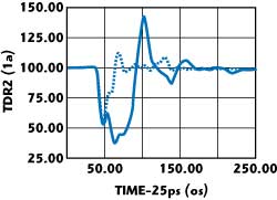
Figure 2 TDR from design in Figure 1a (solid) and b (dashed).
In the lab this behavior is identified through the TDR measurement technique. Figure 2 shows the corresponding TDR plot from the analyses described in Figure 1. The responses align through the microstrip transmission line until reaching the stripline breakout layer where the design without back drilling exhibits a sharp and undesirable capacitive response in the TDR.
Finite Element – Boundary Integral
Inspired by recent advancements in domain decomposition techniques, a new hybrid finite element/integral equation technique is introduced in HFSS 13.0 for modeling large unbounded radiation and scattering problems. This technique, more commonly referred to in the literature as finite element-boundary integral (FE-BI), effectively truncates a nominally bounded finite element solution with a boundary integral. In HFSS 13.0 this new truncation is implemented as a full-wave integral equation, i.e. method of moments solution that satisfies the Sommerfeld radiation condition at infinity. This effectively utilizes the two simulation techniques, FEM and MoM, in their respective areas of strength; finite elements for handling complex geometries, materials and excitations and method of moments in solving directly for surface currents satisfying an open boundary problem. Engineers are able to model much larger systems such as antenna placement or radar cross-section studies.

Figure 3 Dielectric lens with rectangular waveguide feed with FE-BI and separate air volumes (left) and traditional PML with all surrounding air volume (right).

Figure 4 Field along line through center of feed antenna and lens for FE-BI model (blue circle) and PML model (red line).
Separate Finite Element Volumes
An interesting aspect of the FE-BI technique is its ability to act as a two- way "field link" between two physically separate volumes. To demonstrate, see Figure 3, which shows a snapshot of the electric fields in a cut plane between a rectangular waveguide radiator illuminating a composite dielectric microwave lens. An FEM only solution would require the simulation of the entire air volume contained between the horn and lens. For the system in Figure 3, however, only the air volume immediately surrounding the radiating horn and lens need to be included in the FEM portion of the simulation. The equivalent surface currents capturing the coupling between these air volumes are computed via the integral equation solver. Thus, the overall computational domain for this system can be significantly reduced through the application of the FE-BI technique. Also note that the separation between the horn and lens may be varied without affecting the computational effort since the FEM volume and IE surface area will not change with separation. Figure 4 is a plot of the electric fields along the center connecting axis of the system in Figure 3. The line represents the fields for a full FEM solution with the entire air volume between horn and lens simulated; the data points represent the same system with the FE-BI technique coupling the fields between separate air volumes.

Figure 5 Backplane in Designer layout interface solved with HFSS SoD.
HFSS – Solver on Demand
Ease of use and accessibility are two very critical aspects of simulation software design. Many electrical engineers are familiar with layout-based design flows for chip package and board design. These designs, although 2D in the nature of their creation, are representations of 3D designs, which at higher frequencies and data rates require a rigorous full-wave 3D simulation. The HFSS Solver on Demand technology enables users to drive HFSS directly from the intuitive parametrically driven stack-up based layout interface of Ansoft Designer (see Figure 5). With Solver on Demand technology, the material properties, port definitions and boundary conditions are set automatically within the Ansoft Designer layout interface. Integration to Cadence Design Systems, Mentor Graphics, Altium, Zuken, Autocad and GDSII support exists through AnsoftLinks.
HFSS version 13.0 introduces new solver technologies and integrated design flows to allow engineers to solve large, more complex designs. HFSS Transient and the new hybrid finite element – boundary integral solvers provide additional insight and higher solution capacity for the toughest electrical design challenges. HFSS Solver on Demand in Designer provides an easy to use layout driven interface for the HFSS solver technology to enable simulation of chip, package and printed circuit board designs generated from layout.
ANSYS Inc.,
Canonsburg, PA
(724) 746-3304
ansysinfo@ansys.com
www.ansys.com