
The RF and microwave components market has seen the introduction of many new technologies over the years. In the early days, RF and microwave systems and subsystems were built using discrete single-function components, connected by semi-rigid or flexible cables. Each component was realized by the most suitable process and technology for its function. Filters were realized as metal cavities or by lumped element devices. Amplifiers were realized by biasing and matching discrete transistors and so on. The total system was large and bulky, and mismatch between components was difficult to predict and compensate for. Such a subsystem is shown in Figure 1.

Figure 1 Subsystem with semi-rigid cables.

Figure 2 Chip and wire amplifier.
One of the technologies used to realize an RF and microwave function is the microwave integrated circuit (MIC). In this technology, a device in bare die form is used with a combination of soft-board (Teflon-based) or hard-board (ceramics, such as alumina) matching and bias networks. The device is connected to the board with a gold or silver ribbon or bond. This technology is also referred to as chip and wire. Such a MIC amplifier is shown in Figure 2.
Along with improvements in the MIC capabilities, more than a single function was integrated to a single MIC component, thus creating the super-component or integrated multifunction module. These super-components enable a designer to get more functionality into a smaller volume, while keeping the component to component matching under control. Such a super-component is shown in Figure 3.

Figure 3 Super-component, MIC technology.
In the super-component world, miniaturization is limited by several factors. First, the bias and control lines, usually fed from the other side of the mechanical housing, consume a lot of space. In Figure 4, a very small device takes up a much larger area due to the hermetically sealed pins and control lines around it. Another limiting factor is the introduction of filters. Since the MIC is planar in construction, the easiest way to integrate a filter into the design is to print the filter on an alumina substrate. However, planar filters have a lower Q-factor than 3-D filters and thus more filters must be used in a given design. Non-planar filters were also used, paying the price of higher volume.

Figure 4 Phase shifter feeding network.
In highly integrated super-components, there are also some DC and digital functions to be integrated. This was usually done by designing a standard PCB, with all components assembled by the automatic surface-mount technology (SMT) process. This DC and control PCB is usually located in the side opposite to the MIC side, with hermetical pins connecting the two sides. This allows the PCB to be located in a non-hermetic space and thus makes it easier for a designer to come up with smaller assemblies.
Along with the introduction of microwave monolithic integrated circuit (MMIC) technology, multifunction devices become available in the form of a single die or SMT device. This enabled reducing the size of super-components even further. By using commercial off-the-shelf (COTS) MMIC devices, several dies may be replaced by one MMIC. For medium and large scale programs, system designers use custom MMIC devices that are designed to meet the exact functionality and size requirements for the specific program. In Figure 5, a custom millimeter-wave tripler with high fundamental signal rejection is shown.

Figure 5 Millimeter-wave tripler.
As MMIC and SMT technologies advance, more and more super-components are realized as pure SMT circuits. Currently, this approach supports the low to medium frequency range. High-frequency or high-Q filters are still a challenge in these non-hermetic all SMT circuits.
In recent years, MIC technology in multilayer RF circuits has emerged as the chosen solution for small form and high functionality integrations. As described below, this technology enables combining bare-die devices, SMT components (including BGA), planar filters, ceramic filters, DC and control functions, and more.

Figure 6 Cavity (zoom-in).
Multilayer Construction
This method comprises multilayer RF and microwave circuits based on PCBs with many different layers of different composition and thickness. Usually the top and bottom layers are used for the RF signals, one or more additional internal layers are used for RF bypass lines and embedded circuits, and the other layers are used for DC and control and various analog functions. The top layer has some cavities in it. The cavities extend down to the ground metallization of the RF top layer. Such a cavity is shown in Figure 6.
An RF device is placed inside the cavity. This can be a transistor, a MMIC device, an alumina filter, etc. The device has excellent grounding since the grounding is common to both the RF feeding lines and the device. Assuming the cavity depth is carefully chosen, the devices do not protrude from the cavity and bonding wire or ribbon lengths are kept to a minimum. By analyzing only the top layer, this looks like a classic MIC assembly, and all the design roles of MIC assembly apply here.

Figure 7 Elisra's DCA in multilayer PCB.
Main Technological Achievements
DC and Control Feeds
As described above, in MIC technology, the DC and control feeds occupy much of the area around the device. In a multilayer circuit, these lines are routed in the inner layers and pop-out, using a via-hole very close to the device. This reduces the required area significantly. In the top layer, above the DC and control line, the area is used for other functions; various active and passive devices may be assembled without interacting with these internal lines. In Figure 7, a digitally controlled attenuator (DCA) is fed by ten differential command lines, with very modest real estate on the board used for that in particular.

Figure 8 Amplifier in a cavity.
Wideband MIC Device Integration
Since the devices are assembled on a common ground with the RF feeding lines and since the bond wire or ribbon length is kept to a minimum, a very wide band of frequencies is supported. Some products cover a frequency range starting at very low frequencies and reaching millimeter waves. The devices, such as MMICs, alumina matching circuits or discrete chips, are attached directly to the bottom of the cavity. Where the devices are very thin, a metal pedestal may be used in order to align the device with the rest of the circuit. This is a common practice in MIC assembly and works just fine for multilayer circuits as well. The measured performance of devices embedded in the multilayer board is compared to these of standard MIC assemblies. An amplifier in a cavity is shown in Figure 8.

Figure 9 BPF in a cavity.
Alumina Passive Devices
Using the cavities for passive devices that are printed on alumina substrates enables a wide range of applications. An SMT board may now include some alumina filters for high frequencies. Wideband alumina couplers, hybrids and other types of circuits are also easily integrated. Since the alumina substrate is placed directly in the cavity and there is no height difference between the lines printed on the alumina and the lines printed on the multilayer board, excellent frequency response is achieved. A BPF on an alumina substrate integrated on a multilayer PCB is shown in Figure 9.
Single-side RF Bypass
As with lower frequencies, it is sometimes necessary to get from one point of the circuit to the other side without interacting with the other components on board. This is done by using a blind via-hole to connect the upper layer transmission line to an inner layer transmission line. For DC and control, only one via-hole will suffice. However, in the RF and microwave world, transmission lines have two parts: the center (or top) line and the ground line (or plane).
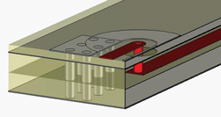
Figure 10 Via-hole microstrip to stripline transition.
Thus, in order to connect a microstrip line on the top to a stripline on an inner layer, the grounding plane must be connected as well. It is therefore required to add more via-holes near the main via-hole in order to maintain grounding continuity. A 3-D model of the transition is shown in Figure 10. The exact dimensions of this transition must be analyzed and optimized, based on the exact dielectric and mechanical properties of the selected layers.
Side-to-side RF Connections
In some multilayer boards, the bottom side is also used for transmission lines, in order to enable more flexibility in signal routing across the board. For that end, a side-to-side connection is used. The design procedures and considerations are similar to that of the single-side RF bypass. However, the resulting dimension after optimization may be different, due to different types and numbers of layers involved. Note that the RF signal is now crossing many layers, each containing different signals. Caution must be used in order to avoid cross-coupling between the RF, DC and control signals. Each layer must be monitored and proximity between RF vias and DC and control lines must be avoided.

Figure 11 Stripline filter on a coupon.
Buried Filters
As described above, filters may be constructed on the top layer as lumped elements or as alumina printed circuits. However, in order to save board space, it may be desired to realize the filters in the inner layers. This is done using a standard stripline type of filter. The filters are fed from the top layer and do not take any of the board real estate. More than one filter may be connected in series in order to improve out-of-band rejection properties. In Figure 11, a coupon of a BPF is shown. Only the input and output transmission lines are visible.
Board Design and Manufacture Challenges
Multilayer board design is not as straightforward as it seems. First of all, the number of layers and their composition must be selected. The top layer, bottom layer and inner RF layer material is chosen. This material must support the highest frequency used within the board with minimum loss.
The thickness of the RF layer must be carefully selected. Thin layers will yield very thin RF lines, which are more difficult to manufacture, have higher loss and are prone to mechanical damage. The thickness of the top layer, where the cavities are realized, must be compatible with the thickness of devices and alumina substrates to be used within the cavities. Once the RF layers have been selected, more DC and control layers are introduced. It is important to keep the board symmetric, so that it does not bend after production and assembly. Sometimes, it is necessary to add an additional layer just to keep the board cross-section symmetric.
The next step is to decide how many types of via-holes are to be used. The more types of via-holes used, the more production steps are needed. This is a major cost and yield factor. Another limitation is that not all via-hole combinations are possible. For example, take an 11-layer board. A side-to-side via-hole is the 1-11 via-hole.
If an internal RF line is used, the designer may want to use the 1-x via-hole, where x is the inner line index. Once a designer has decided on that, it is not possible to use a y-11 via-hole if y has values between 1 and x. Thus, it is impossible to manufacture such a circuit. What is easily possible with LTCC circuits becomes a limitation in multilayer technology.
Once all the layers are selected and all the via-holes are defined, a survey of manufacturers must be conducted. Not all PCB manufacturers can handle RF cavities. In the standard PCB world, if some adhesive film spills out from inside the board to the cavity, this is not a critical issue. However, for RF assemblies, this may cause the alumina circuits or discrete components to be unleveled and have poor grounding. The cavities must have a perfectly clean metal bottom and perfectly straight walls, as seen in Figure 6.

Figure 12 DIFM unit.
Product Examples
Wideband DIFM
The wideband digital instantaneous frequency measurement (DIFM) module (Elisra Microwave Division) is a wideband receiver. This receiver covers the 2 to 18 GHz instantaneous bandwidth. Any signal, from a short 100 nanoseconds single pulse up to CW within this frequency range, shall be detected and its frequency shall be measured. The frequency measurement has a resolution of 0.9 MHz with an accuracy of 2.5 MHz RMS. The DIFM covers 60 dB of dynamic range, down to signal levels of -55 dBm. The DIFM is capable of accurately measuring the signal's frequency within a SNR of 3 dB. The module is housed in a 152 × 147 × 30 mm package and dissipates 24 W. The RF side of the module is shown in Figure 12.
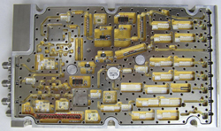
Figure 13 Narrow band receiver.
Narrow Band Receiver
The narrow band receiver (NBR) module is a classical superheterodyne receiver. This receiver covers the 0.5 to 18 GHz band and may zoom in to any required sub-band with various IF bandwidths. The NBR covers 80 dB of dynamic range, down to signal levels of -75 dBm. Once a threat is detected, the NBR jumps to that sub-band within 50 nanoseconds. The signal is converted to a video signal for amplitude measurement and converted to the IF frequency for further analysis. The module is housed in a 152 × 147 × 30 mm package and dissipates 24 W. The module is shown in Figure 13.
Future Trends
As MMIC packaging techniques improve, more devices are becoming available in the SMT package for increasing frequencies. This enables multilayer circuits to contain more SMT devices and fewer cavities. This trend reduces the cost of the module. However, the size of the module may be affected, since the SMT device may need more real estate on the board than a die component in a cavity.
One current area of research is substrate integrated waveguide (SIW) components. Using this technique, some of the alumina filters may be replaced by SIW filters. Another trend is that both sides of the PCB are used for RF with cavities. This enables twice as much area on board for die and alumina circuits. However, the cost and the yield of the PCB and the assembly costs become higher.
As system designers push for more functionality in ever decreasing volumes, engineers are going to come up with new and creative ways to accommodate this need. Multilayer is just one more step in this direction.
All the photos in this article are courtesy of the Elisra Microwave Division.
Ronen Holtzman is a Senior Scientist in the CTO Division of Elisra Electronics Systems Ltd. He has more than 20 years experience and is a specialist in RF and microwave super-components and subsystems.