

In this installment of our blog series about Power Supply Ripple Rejection, we’ll take a break and shift our focus from PSRR to output impedance ZOUT.
Before the 21st century, most voltage regulator datasheets started their electrical characteristics (EC) tables with two key parameters:
- Line Regulation
- Load Regulation
For example, the LM317 datasheet of the early days [1] started its electrical characteristic table with the values as seen in Table 1:
 Table 1: LM317 specifications for load and line regulation
In the previous parts of this blog series from Part 3 to Part 5, we reviewed various aspects of line regulation ΔVOUT/ΔVIN and PSRR. Now we move our focus to their counterparts; load regulation ΔVOUT/ΔIOUT and output impedance ZOUT.
In a very simple way, near DC, we use the arrangement of Figure 1 to consider a power line voltage drop VO, due to current through its output resistance RO.
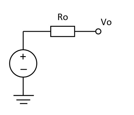
Figure 1: Simple Voltage Source with an Output Resistance RO
This resistance RO is not necessarily a discrete component - the parasitic resistance of a length of PCB trace has the same effect.
Between the years 2005 and 2010, CPU supply current began to exceed 100 A. At this high current flow, just 1 mΩ of PCB trace (parasitic) resistance produces 0.1 V drop between a VRM and the CPU. When the CPU core voltage is only around 1 V, this represents a 10% voltage error.
Between the years 2005 and 2010, CPU supply current began to exceed 100 A. At this high current flow, just 1 mΩ of PCB trace (parasitic) resistance produces 0.1 V drop between a VRM and the CPU. When the CPU core voltage is only around 1 V, this represents a 10% voltage error.
While many CPU devices have remained around this 100 A current milestone, the use of GPU chips has been growing and has quickly reached the position of most power-hungry category of ICs. Today, many GPUs consume one half kilowatt (500 W), and we do not see signs of a slowdown in their increase in current demand.
How to feed CPUs and GPUs is the main discussion of Power Delivery Network (PDN) impedance, and a low value is one of the foundations for power-integrity considerations.
To provide a well-regulated voltage supply for CPUs and GPUs, various circuit techniques are used:
- VRMs sense the output voltage very close to the load processor devices
- VRMs sense the output voltage return (e.g. ground) at the devices as well, to form a differential sensing pair
- A PDN-impedance design flow adds bypass capacitors placed at right position and with the right values.
Starting from the simple diagram of Figure 1 with a voltage source and an output resistor, I tried to visualize the two parameters: PSRR and ZOUT in a linear regulator (Figure 2, top) and in a switching regulator (Figure 2, bottom).
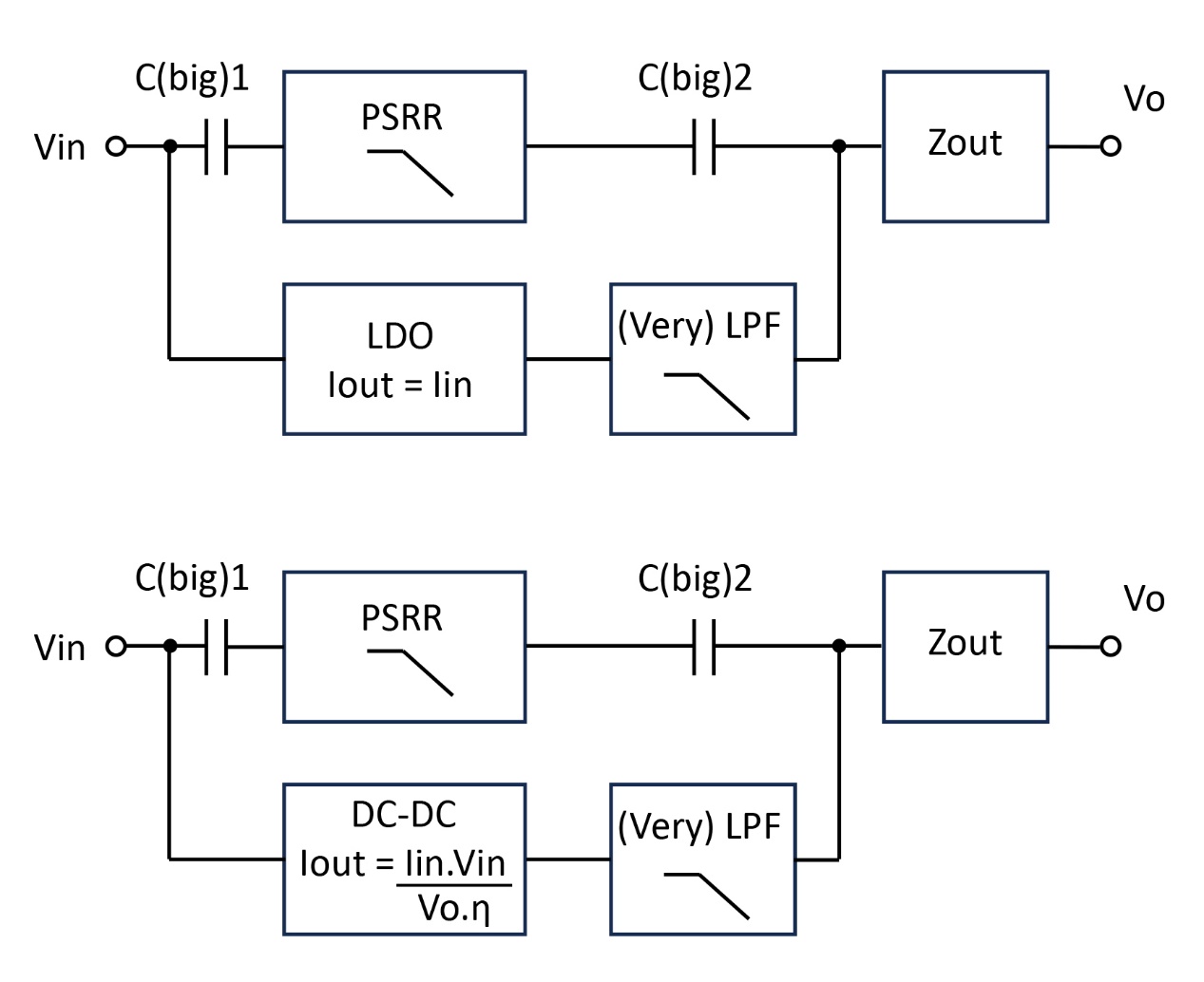
Figure 2: PSRR and Zout in a linear (top) and switching regulator (bottom)
In the two diagrams, the LDO and DC-DC blocks correspond to ideal voltage sources. As our frequency domain performance is represented by the PSRR block, we limit these LDO and DC-DC blocks to very low frequency with the (very) low pass filter. Then, the output resistance is re-labeled as ‘ZOUT’ as our interest now extends into the frequency domain.
For engineers working in signal chain or RF designs and applications, the below Table provides an analogy [2] that will make it easier to understand on why PSRR and ZOUT are the top two key parameters. These metrics can be seen as equivalent to ‘S’ parameters (Table 2).
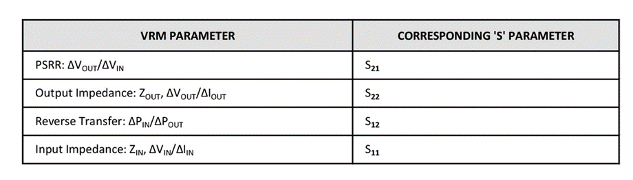 Table 2: VRM and ‘S’ parameter equivalence
These cannot be ‘true’ S-parameters, because we are considering power supplies (that is, VRMs) and we cannot use 50 Ω (or 75 Ω) as our reference impedance for these power parameters. However, the concepts of measurement are the same.
The S-parameters are a set of four, where S21 corresponds to PSRR and S22 to ZOUT. The other two are:
- S12 – reverse transfer function representing any dynamic event showing up at the upstream supply
- S11 – input impedance, which defines required upstream supply strength
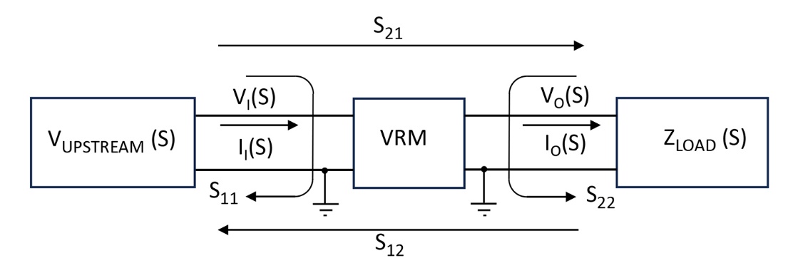
Figure 3: S-Parameter equivalence to power parameters, analogy
(Readers who checked Part 3 of these blogs can skip the following section.)
We can find load regulation curves in most VRM datasheets, as in the example of Figure 4.
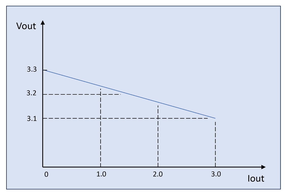
Figure 4: A VRM example load regulation curve
Behind the scenes, the above production data curve must consist of multiple actual measured data points as in the dots in the raw plot in Figure 5.
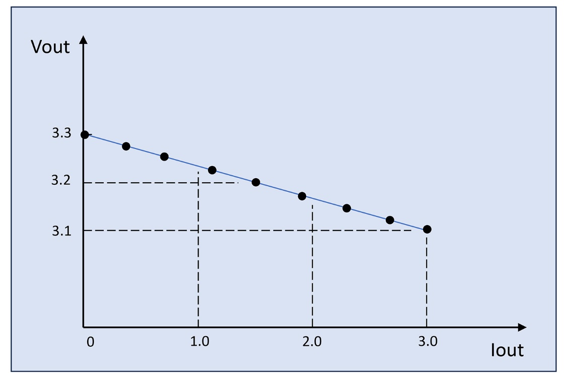
Figure 5: Load regulation curve with data-points
When we think of how engineers find these data points during bench testing, they must have swept the load current ILOAD by turning the knob of an electronic load (e-load) unit. By plotting this operation in time, we get the data points as in Figure 6. For the following discussion, let us assume it took 10 seconds between logging data points.
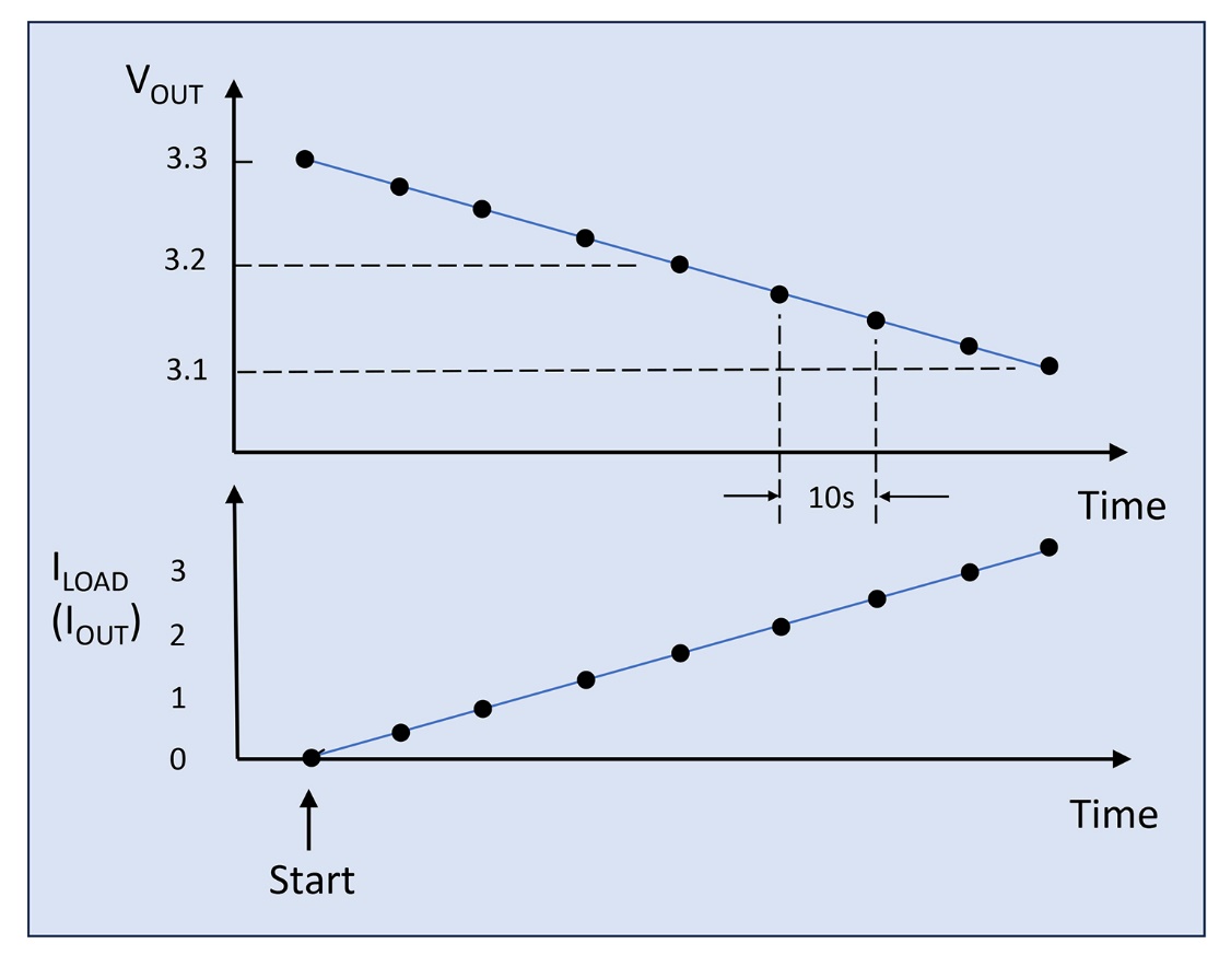
Figure 6: Load regulation data as taken at a bench over time
Now, if the time scale is compressed, we can approximate the plot of Figure 6 to part of a bigger sinusoidal ILOAD sweep, though only half of a period (bottom peak to top peak). This will lead us into Figure 7.
The portion measured consists of nine data points from peak-to-peak. With our assumption of 10 seconds between each point, this gives about 90 seconds for this half cycle, or a total of about 180 seconds for the full sinusoid. We can say this this load regulation curve running a 5.6 mHz VIN sweep in the frequency domain.
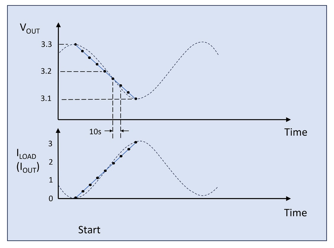
Figure 7: Load regulation data points expanding to a sine wave approximation
When the engineer decides to program their measurement process in an automated characterization system, this ILOAD sweep can be faster, and it could be perhaps 100 ms between data points. Then, the sweeping frequency becomes 0.56 Hz. When we use an IC testing machine to check this linear regulator in its production test, this sweeping frequency goes much higher, into the 100 Hz range.
Now, we can plot the ‘ΔVOUT / ΔILOAD’ parameter at different frequency sweeping rates, yielding an output impedance ZOUT curve in the frequency domain.
Figure 8 reiterates the definition of ‘DC load regulation’ and Figure 9 represents one frequency point of ZOUT. From the above step-by-step illustrations, we can see that these two graphs illustrate the same VRM performance but from different viewpoints.
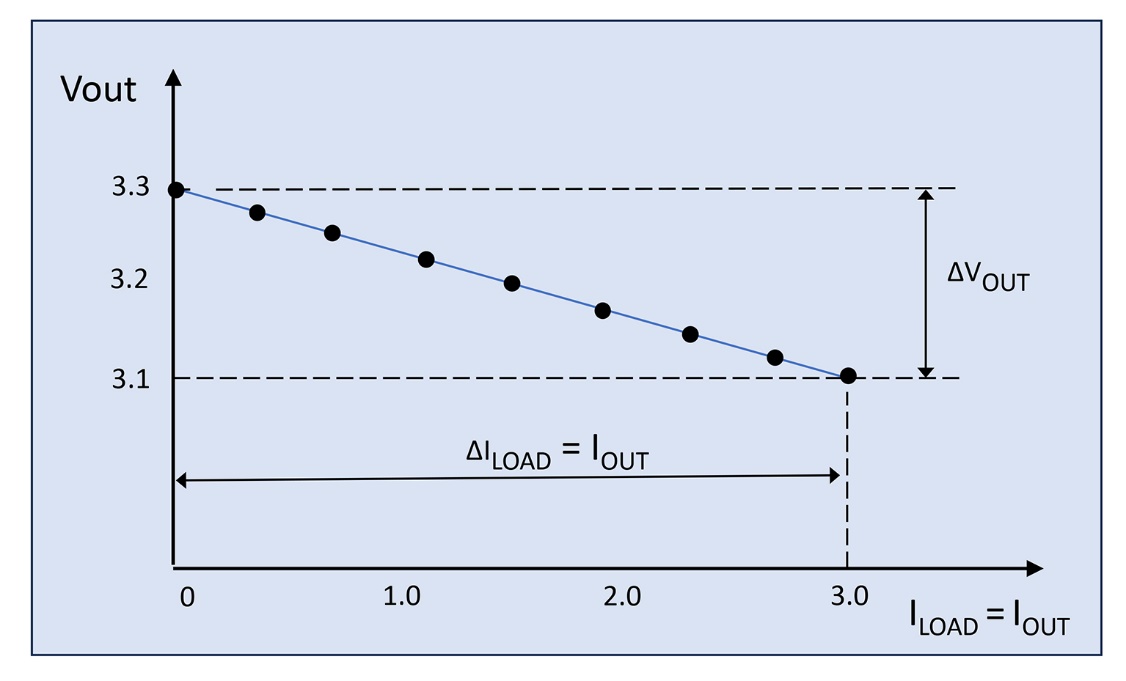
Figure 8: DC load regulation re-iterated
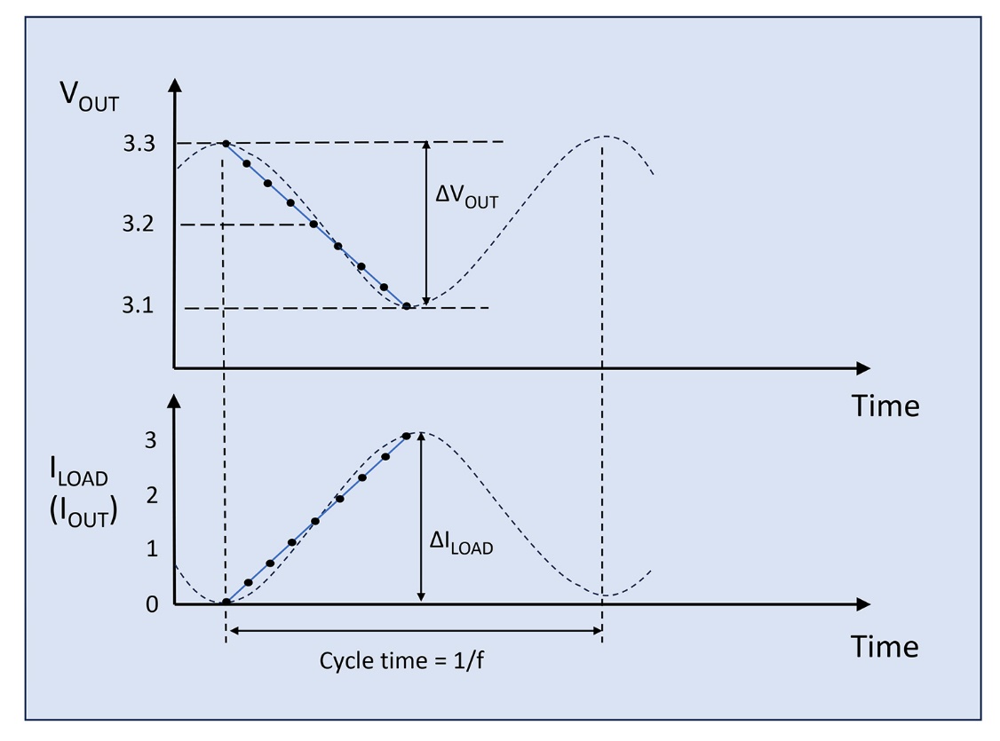
Figure 9: Definition of ZOUT = ΔVOUT/ΔILOAD at one frequency point ‘f’
[1] Voltage Regulator Handbook (National Semiconductor, 1980, pp. ‘10-8’ to ‘10-15’)
[2] Measurement Based VRM Modeling (Steve Sandler, PicoTest, 2017, page 4)