
.webp?t=1681474360)
THE POTENTIAL OF GAN HEMTS FOR MMWAVE MOBILE COMMUNICATION
As the demand for bandwidth continues to grow and existing radio spectrum bands get congested, the telecom industry is looking for novel technologies to meet the requirements for future mobile communication. The quest for more bandwidth is inextricably linked with the use of higher radio frequencies and higher operating frequencies mean more available bandwidth. While researchers examine new III-V materials such as indium phosphide for frequencies above 100 GHz, they expect GaN-based technology to play a significant role in the lower mmWave part (i.e., below 50 GHz) of the RF spectrum. Because of this, GaN is expected to serve the next generation of 5G networks and possibly, early versions of 6G.
GAN ADVANTAGES
GaN technology owes its potential for RF/lower mmWave communication to its outstanding physical properties: it has high current density, high electron mobility and high breakdown voltage. The technology can handle switching frequencies higher than today’s Si-based technology because of its high mobility. Beyond speed, GaN-based technology is touted for its power handling capabilities, which make it capable of delivering high output power with good energy efficiency. These features can make GaN an attractive technology to use in the power amplifiers (PAs) that reside in the front-end modules of next-generation mobile handsets and small cells. These front-end modules send the RF signals to and from the antennas. The higher power handling capabilities of GaN compared to conventional Si- or SiGe-based technologies translate into a higher transmission range and/or into a smaller number of elements needed to drive the antennas.
REDUCING FORM FACTOR AND COST: TOWARDS A VIABLE GAN-ON-SI TECHNOLOGY PLATFORM
To be suitable as a PA in user equipment and small cells, the cost and form factor of the device can become as important as its electrical properties. As stated before, GaN helps reduce the form factor of the front-end module thanks to the inherent properties of the technology. But achieving highly-scaled form factors requires integrating the miscellaneous components of the RF front-end technology. To help achieve this goal, imec is tuning its GaN-on-Si technology platform towards RF applications, as part of its Advanced RF program.
imec has selected GaN-on-Si rather than GaN-on-SiC for cost-saving reasons: not only are Si substrates cheaper, but the CMOS-compatible process also enables large-scale manufacturability. GaN-on-Si technology was initially developed for power electronics applications and envisioned to enable power conversion within battery chargers, computers, servers, automotive, lighting systems and photovoltaics. However, several technology innovations are required to make GaN-on-Si suitable for mobile RF applications. Parasitics within the device structures must be suppressed as much as possible to reach high frequencies. Examples of these efforts include reducing the source access resistance with methods like developing technology modules with raised source/drains and reducing gate-related parasitic capacitances. Optimizing the device for higher operating frequencies will also require a further downscaling of the gate length. This benefits a higher fT and fmax, which is a measure of the intrinsic speed of the device. Furthermore, the buffer layer must be made RF-compatible to minimize the RF substrate losses.
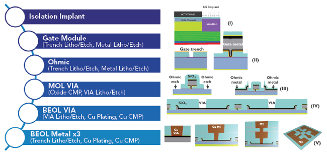
Figure 1 Three-level Cu back-end-of-line process flow for GaN-based mmWave devices.
imec’s GaN-on-Si process flow for RF starts with the metal-organic chemical vapor deposition growth of an epitaxial structure on 200 mm Si wafers. The epitaxial structure is comprised of a proprietary GaN/AlGaN buffer structure, a GaN channel, an AlN spacer and an AlGaN barrier. GaN HEMT devices with TiN Schottky metal gate are subsequently integrated with a low temperature three-level Cu back-end-of-line process as shown in Figure 1. imec researchers used this CMOS-compatible platform to fabricate GaN HEMTs, as demonstrated at the 2020 International Electron Devices Meeting (IEDM 2020). Optimizations of the gate metal stack, contact resistance and gate length scaling up to 110 nm resulted in devices with an fmax of 135 GHz, which represents a step forward towards mmWave applications. Key figures of merit for PAs are the output power and the efficiency that the transistors can deliver. Competitive results are obtained on imec’s GaN-on-Si platform, reaching a power-added efficiency (PAE) of 60 percent and a saturated power output (PSAT) of 2 W/mm for an 0.19 μm gate length (LG) device at 6 GHz. These results, presented at European Microwave Week 2022, are shown in Figure 2a. Figure 2b, presented at IEDM 2022, benchmarks the performance of the imec GaN-on-Si process versus other GaN-on-Si and GaN-on-SiC processes. The imec data in red is among the best reported for GaN-on-Si devices and comparable to GaN-on-SiC devices. Using shorter gate lengths improves the measured performance at 28 GHz. With these improvements, imec believes that the PAE of amplifiers designed to meet user equipment requirements and fabricated with a GaN-on-Si process achieve parity with equivalent GaN-on-SiC amplifiers for the first time.
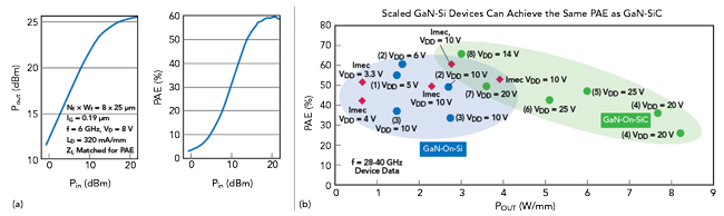
Figure 2 (a) Large signal performance of imec’s GaN-on-Si transistors. (b) GaN-on-Si benchmarking data.