
This article presents the design approach and test results of a X-/Ku-band 4-bit compact GaAs MMIC phase shifter developed for broadband applications. The phase shifter design is based on choosing an optimum topology for each bit, yielding compact size and low insertion loss. It also has on-chip integrated digital control. The MMIC phase shifter was fabricated employing GaAs-based high-performance 0.4 μm multi-function self-aligned gate (MSAG) MESFET technology with a multilevel plating process. A chip size of 2.6 mm2 was achieved, the smallest size reported to date, and the MMIC phase shifter demonstrated state-of-the-art performance.
Several X-/Ku-band applications require multi-bit compact and low-cost phase shifters. For example, beam scanning in electronically-steered antennas is achieved by changing the phase of the RF signal fed to or received from each radiating element. For beam steering, programmable and digital bidirectional-phase shifters are required to adaptively adjust the transceiver phase in both transmit and receive modes. Generally, the digital bits in a multi-bit phase shifter have binary values, that is 4-bit and 5-bit phase shifters have 180°, 90°, 45°, 22.5° bits and 180°, 90°, 45°, 22.5°, 11.25° bits, respectively.
Most practical electronically-steered antennas for commercial applications, including satellite communication and WiMAX base stations, use 4-bit phase shifters as a compromise between cost, size, insertion loss and the incremental improvement in system performance when more phase bits are used. Large antennas rely on compact and low cost monolithic programmable multi-bit phase shifters based on FETs to achieve minimum size, weight, power consumption and cost.
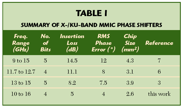
During the past decade, there has been significant progress in programmable phase shifters. Many different technologies such as GaAs MESFET MMIC1–3 and Si-based MMIC,4–7 including MEMS,4 SiGe p-i-n diode,5 MOSFET6 and CMOS7 are being pursued to develop compact and low cost phase shifters. Progress in X-/Ku-band multi-bit MMIC phase shifters is summarized3–7 in Table 1. It may be noted from this table that, in comparison to GaAs-based MMIC phase shifters, the Si MMIC phase shifters have much higher insertion loss because of the lower resistivity of bulk silicon.
This article reports on the design and test results of a compact and low loss X-/Ku-band 4-bit GaAs MMIC phase shifter. The MMIC has on-chip integrated digital drivers for low cost applications.
Phase Shifter Design
Excellent multi-bit L- and S-band phase shifters for octave band applications have been developed using the GaAs MSAG MESFET process.8,9 In order to meet current requirements and gain wider acceptance, MMIC phase shifters must have a small size and low insertion loss. These features can be accomplished with the MSAG process, using M/A-COM’s Process 5C FETs with multi-level plating (MLP), high Q inductors9–11 and a 5-mil thick GaAs substrate. The insertion loss can be further reduced using a suitable topology with fewer devices connected in series, while size is reduced by careful selection of topology, compacting components and MLP. The MLP process enables the incorporation of multi-layer microstrip lines and also provides flexibility in routing control bias lines in a compact way.
Digital phase shifters can have a number of topologies,12–19 but the general principle is either the signal is switched between two separate networks, which have a fixed phase difference, or the phase shift of a single network is controlled by switching elements in or out. There are six main types of solid-state digitally controlled phase shifters, each with its own limitations. These are switched line (narrow band), reflection (poor match), loaded line (suitable only for small bits), switched low-pass/high-pass (high loss), switched network (suitable only for 180° bit) and embedded-FET type (suitable only for small phase bits). Generally, a different technique is optimum for each ‘bit’ and also depends on the bandwidth.
In general, the insertion loss of SPDT-based phase shifters is high because the switching devices are in series with the transmission path and the insertion loss increases with frequency. Multiple sections of series/shunt lumped elements results in smaller size and larger bandwidth at the cost of increased insertion loss due to the low Q of these elements as compared to distributed circuit elements such as microstrip. In order to further reduce the size, it has been shown that FET switches can be directly integrated into the filters, and the FET parasitic capacitances can be absorbed into the filter network.12–15
Switching Devices
MESFETs or simply FETs are used as passive two-terminal switching devices, with the gate terminal acting as a port for the control signal only. The RF connections are made to the drain and the source terminals and the gate terminal looks into an open circuit for the RF signal. The RF impedance between the drain and the source terminals depends upon the DC control voltage at the gate terminal. For switching applications, low-impedance and high-impedance states are obtained either by making the gate voltage equal to zero or by using a gate voltage greater (numerically) than the pinch-off voltage, respectively. In most applications, the gate control voltage is approximately 1.5 to 2.0 times the pinch-off voltage (however, for a high power application the control voltage is much higher than the pinch-off voltage) and it is applied to the gate through a resistor which isolates the RF between the FET and the power supply. The resistor value depends upon the FET’s gate periphery and the frequency of operation. For X- and Ku-band switches its value is approximately 3000 Ω-mm, that is, if the gate periphery is 1 mm, the resistor is approximately 3 kΩ.
FET switches are bi-directional, offer wide bandwidth performance and great design flexibility. As they are compatible with GaAs MMIC technology, they have small size, low cost and light weight. They offer:
• Virtually no DC-control power dissipation
• Nanosecond switching speed
• No DC blocking capacitors
• Multi-watt power handling capability
Switching FETs are modeled by two lumped element equivalent circuit models: one when the device is “ON” (low-impedance state) and the second when the device is “OFF” (high-impedance state). The model parameter extraction is generally based on statistical data with average and standard deviation values that will help in centering designs for high yield. A simplified equivalent circuit (EC) model for a MSAG 5C FET is shown in Figure 1. The model element values shown are normalized to 1 mm of gate periphery.
Circuit Design
The X-/Ku-band 4-bit phase shifter was designed with 22.5°, 45°, 90° and 180° phase states. A suitable topology was selected for each bit to provide optimum performance and size. The topology was then optimized, employing the FET model shown with the FET periphery as a variable. Finally, the circuit was re-optimized using measured S-parameters data for FET sizes closest to standard FET cells, that is 50, 75, 100, 150, 200 μm, etc.

During the design of the compact and low-loss phase shifters, several trade-offs were considered, including:
• Insertion loss
• Insertion loss ripple
• RMS phase error
• VSWR
• Size
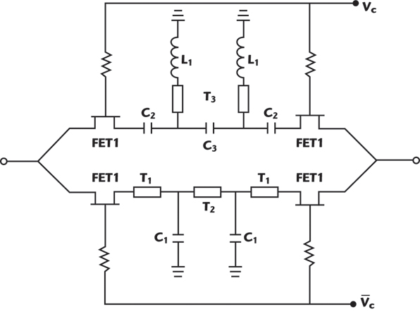
The topology used in the 22.5° bit is of the integrated or embedded-FET type, as shown in Figure 2, where the FET’s reactances become part of the phase shifting low-pass/high-pass filter networks. Here, for the reference state, FET1 and FET 2 are “ON” and FET3 is “OFF.” This configuration has a lower insertion loss due to a single device in series. The configuration for the 45° bit is a modified version of the embedded-FET type topology. Resistor R1 is used to minimize the difference in insertion loss between the ‘reference’ and bit ‘ON’ states. This bit functions the same way as the 22.5° bit.

In order to achieve low insertion loss and a 90° flat phase response, a reflection-type phase shifter topology shown in Figure 3 is used. For broadband applications a Lange coupler is usually used as a 90° hybrid. Signals from the coupled and direct ports are reflected with a magnitude of unity and the resultant signal appears at the output port. The 90° phase shift is achieved by switching in and out capacitor C1. A major problem with this topology is not having a good match over a large bandwidth. In order to get a good match and a flat phase response, the Lange coupler was modified. The Lange coupler’s conductors were placed on 3 μm thick polyimide atop the base GaAs. This configuration results in lower loss and better match than a Lange coupler on GaAs.
The 180° bit design is of the switched low-pass/high-pass filter phase shifter type shown in Figure 4. This design employs SPDT switches to switch the signal between a high-pass and a low-pass filter. The filters have equal amplitude responses over the range of interest. The low-pass/high-pass phase shifter configuration is very suitable where an octave bandwidth and compact size are required.
On-chip Integrated Digital Control
To obtain high-speed operation with low-power dissipation in the FET switches, the phase shifter ICs have integrated on-chip drivers. The primary objectives of the on-chip drivers include: (a) to be compatible with TTL logic levels; (b) minimum GaAs chip size; (c) achieve the same or better chip yield; and (d) to maintain overall lower cost. In these drivers, both depletion-mode and enhancement-mode transistors are used. The logic gate design is generally optimized by adjusting the sizes of the FETs and voltage shift diodes to achieve the correct voltage levels, low power consumption and high speed operation. The design of such drivers is accomplished by using the SPICE program. These drivers are compatible with CMOS and TTL logic families and their treatments have been described by Bahl.11 The power supply voltage VEE for the digital circuits is –5 V and the logic input voltage is 0 V for “low” and 5 V for “high.” The logic inputs are converted to VC and  to drive the switching FETs. The device control voltages are –4.8 and 0 V.
Circuit Fabrication
The phase shifter circuit was fabricated using the ion-implanted planar refractory gate, multi-function self-aligned gate MESFET MMIC process.8 This process features a full suite of active and passive components fabricated on 4" diameter GaAs wafers and is being used to develop low-cost, high-volume, high-performance and highly reliable multifunction monolithic ICs for commercial and military applications. Because of its versatility in integrating microwave and high-speed LSI functions on a single chip, the process has been named the multifunction self-aligned gate process. The MSAG process eliminates the need for a gate recess, the single most important yield and reproducibility limiting step.
Each device type, which may include EFET, DFET, Schottky diode/limiter, low-noise FET, switching FET, power FET and n' implants, is optimized for its respective function. The phase shifter devices were fabricated using a process with three implants. The process includes Au/Ge/Ni metallization for ohmic contacts, 0.4 μm TiWN Schottky barrier gates, along with thin film and ion-implanted resistors. The 0.4 μm TiWN gates are covered by a 0.8 μm overlay after planarization. The MSAG TiWN gate is extremely robust (survives 900°C rapid thermal anneal temperature), which results in an MTTF of 100 years at a channel temperature of 150°C. A thickness of 2000 Å silicon nitride (εr = 6.8) is used for both MIM capacitors and passivation. The air bridges and bonding pads are 4.5 μm-thick plated gold.
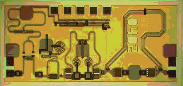
In the MLP MSAG process, three layers of polyimide (εr = 3.2) are used, including inter-level dielectric (3 μm thick), inductor crossover layer (7 μm thick) and scratch protection buffer layer (7 μm thick) for mechanical protection of the finished circuitry. The three metal layers are metal 1 (0.5 μm thick), first plated gold (4.5 μm thick) and second plated gold (4.5 μm thick). The multi-level plating (MLP) process allows the designer to reduce the overall chip size and lower the resistive loss in passive components. Low capacitance metallization crossovers are achieved by a polyimide inter-metal dielectric layer. The front side processing is completed by depositing a polyimide buffer layer. The buffer layer provides mechanical protection of the circuit structures during backside processing, dicing and subsequent assembly operations. Finally, the wafers are thinned to their final thickness, through-wafer vias are etched and the backside is metallized. The substrate thickness of the phase shifter chips is 125 μm. Figure 5 shows a photograph of the X-/Ku-band phase shifter IC. The chip size is 2.4 x1.1 mm (2.6 mm2).
Test Data and Discussions
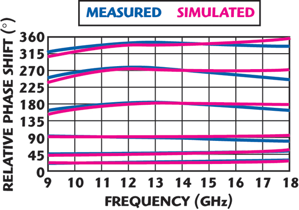
The typical performance of this X-/Ku-band phase shifter was determined using on-wafer measurements to develop the performance charts included in this article. Figure 6 demonstrates the tight correlation between the simulated and measured phase shift versus frequency, particularly over the design band of 10.7 to 15.5 GHz. The phase states shown are reference state, or all phase bits off; all primary bits: 22.5, 45, 90 and 180° and two combination states: 270° and 337.5°, the all-phase-bits on state. This collection of phase states yields a concise representation of the IC performance without the overhead of measuring and analyzing every phase state combination.
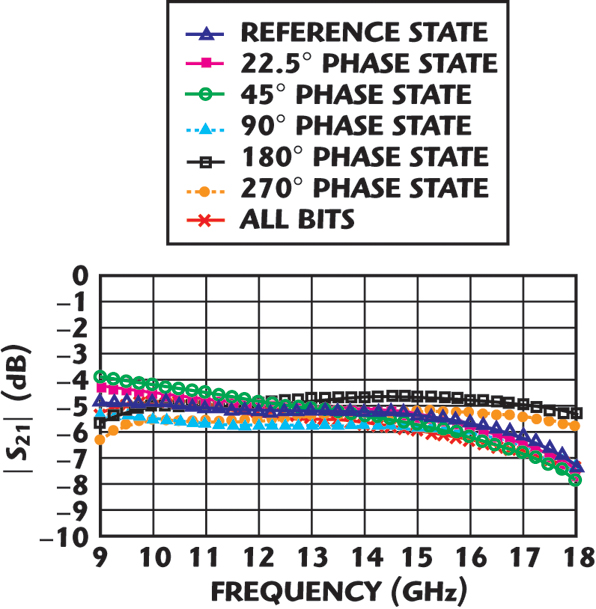
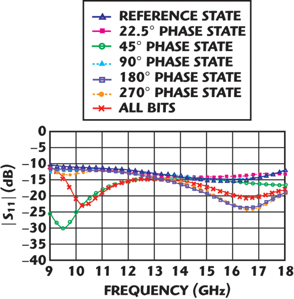
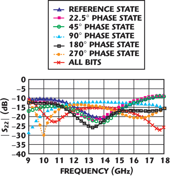
The insertion loss, input return loss, and output return loss versus frequency and phase state are shown in Figures 7, 8 and 9, respectively. Over the design band, the insertion loss of the X-/Ku-band phase shifter is excellent at less than 6 dB. In addition, the gain variation with respect to phase state is also quite good at less than 1.5 dB, or an RMS amplitude error of less than 0.3 dB. The S11 and S22 magnitudes (input and output return loss) of this IC are less than –10 dB over all phase states.
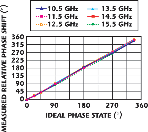
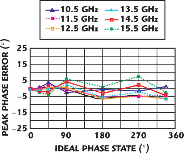
The phase performance metrics of the X-/Ku-band phase shifter are shown in Figures 10, 11 and 12. The normalized phase shift of the device is shown as a function of frequency and commanded phase state. These figures demonstrate the high degree of phase accuracy across the entire design band. This behavior is borne out in further detail when the measured phase shift is compared against the ideal phase value. The worst case, or peak phase error, over the tested phase states and frequencies is –6.0° to 8.0°.
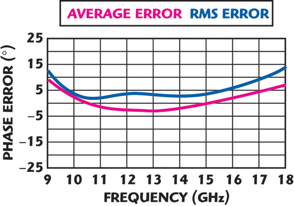
Finally, the average phase error and the RMS error for this phase shifter are shown. The average error is between –2.5° and 1.0°. The RMS phase error is less than 4° across the operating band. Taken together, the peak, average, and RMS phase errors are indicative of a very good, mature phase shifter design. However, these results were achieved on a first iteration with minor tweaks. The performance outcome of this X-/Ku-band phase shifter is a strong validation of the topologies and methodologies employed in the execution of this design.
Conclusion
At these error levels, this phase shifter could be used in most phased-array applications without a look-up table. A look-up table is a mapping used to minimize the error between the actual phase shift and the commanded phase state. This fact results in a greatly simplified aperture calibration process and less overhead in terms of physical memory employed in the aperture beam steering processors.
Acknowledgment
The authors wish to acknowledge the support of M/A-COM’s layout, test, standard microwave products and wafer-processing groups.
References
1. H. Hayashi and M. Muraguchi, “A MMIC Active Phase Shifter Using a Variable Resonant Circuit,” IEEE Transactions on Microwave Theory and Techniques, Vol. 47, No. 10, October 1999, pp. 2021–2026.
2. C.F. Campbell and S.A. Brown, “A Compact 5-bit Phase Shifter MMIC for K-band Satellite Communications Systems,” IEEE Transactions on Microwave Theory and Techniques, Vol. 48, No. 12, December 2000, pp. 2652–2656.
3. W.J. Chang and K.H. Lee, “A Ku-band 5-bit Phase Shifter Using Compensation Resistors for Reducing the Insertion Loss Variation,” Electronics and Telecommunications Research Institute Journal, Vol. 25, No. 2, February 2003, pp. 19–24.
4. S. Lee, J. Park, H. Kim, J. Kim, Y. Kim and Y. Kwon, “Low-loss Analog and Digital Reflection-type MEMS Phase Shifters with 1:3 Bandwidth,” IEEE Transactions on Microwave Theory and Techniques, Vol. 52, No. 1, January 2004, pp. 211–219.
5. M. Teshiba, R.V. Leeuwn, G. Sakamoto and T. Cisco, “A SiGe MMIC 6-bit PIN Diode Phase Shifter,” IEEE Microwave Wireless Components Letters, Vol. 12, No. 12, December 2002, pp. 500–501.
6. H.D. Lee, D.W. Kang, C.H. Kim and S. Hong, “A Ku-band MOSFET Phase Shifter MMIC,” 2004 IEEE MTT-S International Microwave Symposium Digest, pp. 191–194.
7. D.W. Kang, H.D. Lee, C.H. Kim and S. Hong, “Ku-band MMIC Phase Shifter Using a Parallel Resonator with 0.18 mm CMOS Technology,” IEEE Transactions on Microwave Theory and Techniques, Vol. 54, No. 1, January 2006, pp. 294–301.
8. I.J. Bahl, M.J. Drinkwine, A.E. Geissberger, E.L. Griffin and J.A. Grzyb, “Multifunction SAG Process for High-yield Low-cost GaAs Microwave Integrated Circuits,” IEEE Transactions on Microwave Theory and Techniques, Vol. 38, No. 9, September 1990, pp. 1175–1182.
9. I.J. Bahl and D. Conway, “L- and S-band Compact Octave Bandwidth 4-bit Phase Shifters,” IEEE Transactions on Microwave Theory and Techniques, Vol. 56, No. 2, February 2008, pp. 293–299.
10. M. Ashman and I. Bahl, “High-performance Wideband MSAG Gain Block/Driver Amplifier MMICs Using MLP Technology,” Microwave Journal, Vol. 47, No. 12, December 2004, pp. 74–88.
11. I. Bahl, Lumped Elements for RF and Microwave Circuits, Artech House Inc., Norwood, MA, 2003.
12. R. Coats, J. Klein, S.D. Pritchett and D. Zimmermann, “A Low-loss Monolithic 5-bit PIN Diode Phase Shifter,” 1990 IEEE MTT-S International Microwave Symposium Digest, pp. 915–918.
13. P. Miller and J.S. Joshi, “MMIC Phase Shifters for Space Applications,” ESA Proceeding of the International Workshop on Monolithic Microwave Integrated Circuits for Space Applications, ESTEC, Noordwijk, March 1990.
14. I.D. Robertson and S. Lucyszyn, Eds., RFIC and MMIC Design and Technology, IEE, London, UK, 2001.
15. S. Marsh, Practical MMIC Design, Artech House, Norwood, MA, 2006.
16. K. Chang, I. Bahl and V. Nair, RF and Microwave Circuit and Component Design for Wireless Systems, John Wiley & Sons Inc., Hoboken, NJ, 2002, Chapter 7.
17. R.N. Hardin, E.J. Downey and J. Munushian, “Electronically-variable Phase Shifters Utilizing Variable Capacitance Diodes,” Proceeding of the IRE, Vol. 48, No. 5, May 1960, pp. 944–945.
18. D.E. Dawson, et al., “An Analog X-band Phase Shifter,” IEEE Microwave and Millimeter-Wave Monolithic Circuits Symposium Digest, 1984, pp. 6–10.
19. K. Miyaguchi, M. Hieda, K. Nakahara, H. Kuruso, M. Nii, M. Kasahar, T. Takagi and S. Urasaki, “An Ultra-broadband Reflection-type Phase Shifter MMIC with Series and Parallel LC Circuits,” IEEE Transactions on Microwave Theory and Technique, Vol. 49, No. 12, December 2001, pp. 2446–2452.

Inder Bahl received a BS degree, an MS degree in physics and an MS degree in electronics engineering. He received his PhD degree in electrical engineering from IIT, Kanpur, India. At M/A-COM, as a Distinguished Fellow of Technology, his interests include device modeling, high efficiency power amplifiers, and MMIC products for commercial and military applications.

Mark Dayton received his BS degree in engineering science from The College of New Jersey in 2000. He joined M/A-COM in 2001, and currently works as a product development/applications engineer in the Commercial Product Solutions Business Unit. His research interests include the design and modeling of microwave and millimeter-wave integrated circuits.