
Improved simulation accuracy is demonstrated using a hybrid electromagnetic (EM) device model, which includes EM wave interaction and coupling effects, versus a piecewise model for a power amplifier (PA) MMIC design.
The use of mmWave frequencies has surged in recent years due to the increased demand for wireless data. Both terrestrial and satellite communication systems continue to push higher into this frequency range to take advantage of the large available bandwidth. While both terrestrial and satellite communication systems will play a key role in our future wireless communication infrastructure, designing the MMICs to support these systems is often challenging. A key component of these wireless systems, and the most challenging to design, is the PA.
For high-power applications at mmWave frequencies, GaN has quickly become the semiconductor technology of choice due to its superior power, and more importantly, linear power performance. This technology also provides high gain and high efficiency while being extremely reliable. While there are many challenges to designing mmWave GaN PA MMICs, this article focuses on the growing challenge of supporting multi-system specifications and how to partition MMICs in simulation for accurate modeling.
MMIC DESIGN FLOW
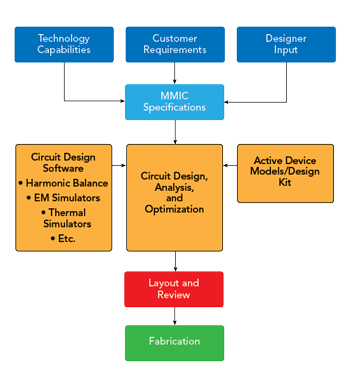
Figure 1 MMIC design flow.
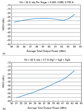
Figure 2 Measured IMD3 with 10 MHz tone spacing at 29 GHz, comparing the PA biased for QPSK (a) and 512-QAM (b) modulation and operating at 25°C.
The common design flow for developing a MMIC is shown in Figure 1. A design starts with collecting information from customers to understand their MMIC needs and system requirements. At this stage, the MMIC designer provides design input, and various semiconductor technologies are assessed to determine the best technology. The goal of this initial stage is to finalize the semiconductor technology and MMIC design specifications.
After these are finalized, circuit design software, which contains various types of simulators (e.g., harmonic balance, EM, thermal and others), is used. Passive and active models for the semiconductor technology are also obtained, most commonly from the semiconductor foundry in the form of a design kit. With these tools in hand, the MMIC designer performs analysis and optimization, in which circuit topologies are analyzed and optimized to achieve the design specifications.
Once the design is completed, it goes through various reviews before the start of fabrication. The cycle time to develop a MMIC typically ranges from six to nine months for design, fabrication and test, but this can vary greatly due to various factors such as circuit complexity and semiconductor foundry lead time. Given the time and cost to develop a MMIC, it is essential for designers to do everything possible to achieve first-pass design success.
SUPPORTING MULTI-SYSTEM SPECIFICATIONS
PA MMIC suppliers develop products to satisfy market demand for a specific frequency band and application. An example is the 27 to 31 GHz Ka-Band used for satellite communications. A portion of this band is also used for 5G mmWave applications.
Within the satellite communications market itself, the requirements for Ka-Band PA MMICs can differ greatly due to the variety of system architectures and designs. One of the main MMIC specifications that varies between systems is the maximum linear power specification, which relates to the linearity of the amplifier.
Linearity requirements are highly dependent on several system-level factors such as the modulation scheme, number of carriers and bandwidth. When different satellite systems have different specifications for PA linearity, it creates a unique and more complicated multi-system specification for the PA. The challenge is to create a MMIC that can support multiple systems, which is more cost effective and profitable for the MMIC supplier.
To illustrate this challenge, consider, for example, the linearity requirements for a QPSK modulation scheme versus a 512 QAM modulation scheme. For QPSK modulation, the maximum output power of a MMIC is commonly specified in terms of a spectral regrowth limit, most typically around -30 dBc. By rule-of-thumb, this would approximate to a two-tone third-order intermodulation distortion (IMD3) specification of -24 dBc. For 512 QAM modulation, the IMD3 specification will be around -45 dBc or possibly lower. Designing a single PA MMIC that provides optimum performance for both these cases is a challenge for the MMIC designer.
Designing PA MMICs to multi-system specifications requires flexible design approaches. One way is to design for multiple biasing schemes. By keeping individual stages of a PA MMIC biased independently and adjustable by the end user, performance can be tailored for different uses. Designing for different biasing schemes requires complex analysis and design work from the onset to determine the best transistor size and total periphery for each stage of the amplifier.
The purpose is to take advantage of the nonlinear effects, namely AM-to-AM and AM-to-PM, of individual stages where the nonlinear effects from one stage of a design can compensate for the nonlinear effects from another stage. This will change based on biasing; and the more gain stages used in a design, the greater the flexibility to accommodate multiple specifications. There are limitations, however, to the number of stages in a PA design, because too much gain can cause stability issues.
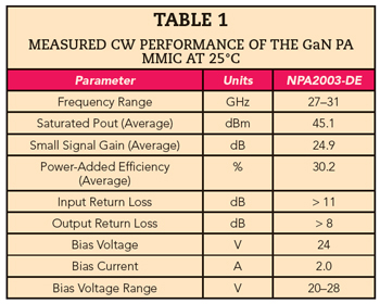
An example of a MMIC designed to operate with different biasing schemes is Nxbeam’s NPA2003-DE. The NPA2003-DE is a 27 to 31 GHz 32 W GaN PA MMIC. Table 1shows the performance of this PA MMIC with the biasing scheme indicated in the figure. To showcase how this MMIC was designed for multi-system specifications, Figure 2 shows the IMD3 results for two different biasing schemes, specifically a QPSK modulation and a 512 QAM modulation.
Figure 2a is the biasing scheme for QPSK modulation. This biasing provides a nulling effect at around 42 dBm output power in which the nonlinear behavior of the second stage of the design compensates for the nonlinear effects from the third stage. By creating this nulling effect, higher output power can be achieved with a smaller output power back-off. From this curve, a power level of greater than 22 W can be achieved for a -24 dBc IMD3.
Figure 2b shows the IMD3 performance for the 512 QAM biasing scheme which is designed to provide a more traditional 3:1 IMD3-to-carrier ratio. It should be noted that the ratio for this MMIC is closer to 2.5:1 in the range of -45 dBc. The figure shows achievable IMD3 levels of -45 dBc or better required for this type of higher-order modulation. At an IMD3 level of -45 dBc, this MMIC provides 4 W of output power.
MMIC PARTITIONING FOR ACCURATE MODELING AND SIMULATION
Once the PA MMIC topology, device sizes and stage periphery ratios have been determined, the challenge moves to accurately modeling and simulating the circuit, which becomes more difficult at mmWave frequencies. Accurate modeling and simulation are critical to achieving first-pass design success. As previously mentioned, MMICs are designed using circuit design software that contains a variety of simulators. Passive components of a MMIC are typically modeled using EM simulators, while the active devices are independently modeled using a variety of different linear and nonlinear models. Some nonlinear model examples include Angelov, Materka and EEHEMT.
Since active device models are independently created, a piecewise design approach is usually taken to design a MMIC. Figure 3 shows an illustration of a piecewise design approach, in which different parts of a MMIC are modeled separately and connected within the circuit design software to simulate the combined circuit performance.

Figure 3 Piecewise MMIC design approach.
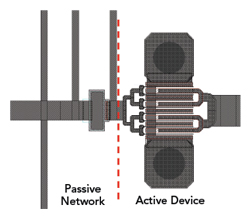
Figure 4 Section of the PA MMIC showing the connection between the passive network and active device.
During the initial phase of a design, lumped or distributed models may be used for the passive components but by the end of the design, EM simulation software is used as it has the capability to capture the true passive network behavior more accurately. With the speed and accuracy of today’s EM simulation software, the entire passive portions of a MMIC can be EM simulated. The final MMIC design will then consist of EM simulated networks of passive components connected directly to the active device models in this piecewise fashion.
To be successful with the piecewise design approach, it is important for the designer to understand how and where to partition a MMIC so that when connected in a piecewise fashion, the correct performance of the circuit is predicted. This partitioning is crucial at mmWave frequencies as passive and active components are moved closer together. Figure 4 illustrates this as it shows a portion of a circuit where an active device is connected to a passive network. The red dashed line represents a common plane to partition this circuit, however, understanding the effects of this partition can affect the outcome.