
To understand circuit partitioning, it is important to look at how these individual piecewise circuit models are created, as well as the assumptions used. Figure 5 shows the passive network from Figure 4. It should be noted that much of the passive network has been removed to simplify this explanation. When simulating a passive structure such as this, it is important to understand what the excitation signal looks like on each port.
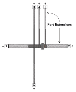
Figure 5 Passive network from Figure 4 used in the piecewise simulation.
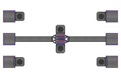
Figure 6 Active device measurement test structure.
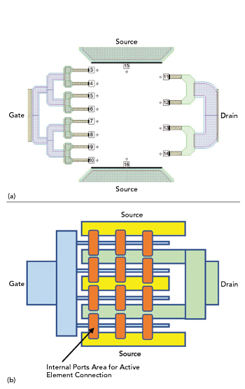
Figure 7 Hybrid EM active device model using grounded port (a) and internal distributed port (b) implementations.
In this case, standard port extensions are used on each port. The purpose of port extensions is to enable any higher-order modes developed from the port excitation method to decay before interacting with the passive structure being characterized. In this way, the resulting S-parameter file will be for a particular excitation mode, mainly the fundamental mode for each port transmission line. When developing a model using this approach, the MMIC designer must understand that the resulting S-parameter model is accurate only for this excitation mode.
Similarly, the development of active device models usually involves taking measurements of a device test structure, like the one shown in Figure 6. As can be seen from the test structure, relatively long transmission lines are used to feed the active device. In this way, the active device is also excited by fundamental mode excitation. Like the EM simulation, the active device model is accurate only for this mode of excitation.
The difficulty with mmWave circuits is that the distance between active devices and the passive structures is short, such that the mode excitation assumed when cascading individual models together may no longer be valid. This is the case shown in Figure 4. The proximity of the discontinuities from the shunt transmission lines close to the input of the active device will generate higher-order modes in that region of the circuit which includes the input of the active device. In this case, there is not enough distance between this discontinuity and the active device to develop a clean fundamental mode excitation. This will be referred to as EM wave interaction and this EM wave interaction must be accounted for in the simulation for accurate circuit prediction.
In addition to EM wave interaction, there are also EM coupling effects that must be considered when partitioning a circuit for piecewise simulation. If elements of the passive EM network are near the active device, this EM coupling may also need to be accounted for in the simulation. An example of this from Figure 4 is the close proximity of the top active device via to the nearest vertical transmission line of the passive network.
A well-documented method to account for this EM wave interaction and coupling effect has been to include more of the active device into the EM simulation.1-3 This is referred to as a hybrid EM device model. Hybrid EM device models have been around for over 20 years with many different styles and implementations. An example of two are shown in Figure 7. The goal of these models is to accurately capture the voltage and current waveform distributions on the active device manifolds or within the active portion of the device.
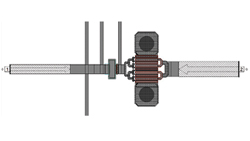
Figure 8 EM simulation of the passive network and hybrid EM device model.
In hybrid EM device models, internal ports are used within the active device that provide the terminals to connect to a core intrinsic device model, such as an Angelov model. Figure 7a shows an example where just the extrinsic device manifolds and source vias are included in the EM simulation. This EM simulation makes use of grounded ports to connect the active device model, while Figure 7b illustrates the use of internal distributed ports for connection to the intrinsic device model.1,2
The challenge with these hybrid EM device models lies in the implementation of the internal ports, which are not true to the real device and will cause their own inaccuracies. The goal however is to develop an internal port method that reduces these inaccuracies such that they have a negligible effect on the surrounding circuitry, or at least less of an effect relative to the EM wave interaction and coupling effects.
With the development of a hybrid EM device model, the EM simulation consists of both the passive structure and the passive portion of the active device model. An example of how the circuit structure presented in Figure 4 would be simulated using a hybrid EM device model is shown in Figure 8. Note that the other ports of the input passive network are not being shown for simplicity.
COMPARISON OF SIMULATION VERSUS MEASUREMENT
To demonstrate improved simulation accuracy using the hybrid EM device model and to show the effect of EM wave interaction and coupling effects, measurements of Nxbeam’s NPA2003-DE are compared with simulations using the hybrid EM device model approach versus the piecewise model design approach. It should be noted that this MMIC was designed using the hybrid EM device model approach. All simulations are done using Cadence’s Microwave Office Design Suite including AXIEM for the EM simulator. All active devices models are developed by Nxbeam.
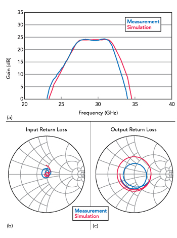
Figure 9 Measured vs. simulated performance, using the hybrid EM device model for the MMIC PA: gain (a) input return loss from 27 to 31 GHz (b) and output return loss from 27 to 31 GHz (c).
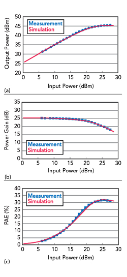
Figure 10 Measured vs. simulated performance at 29 GHz, using the hybrid EM device model for the MMIC PA: output power (a), power gain (b) and PAE (c).
Figure 9 shows small-signal measurement of the NPA2003-DE versus simulation for just the hybrid EM device model approach. As can be seen from the gain in Figure 9a, the hybrid EM device model accurately predicts the gain and bandwidth of the MMIC with a slight exception in the high-end roll-off. The return loss comparisons in Figures 10b and c are included for completeness.
Achieving good agreement between measured and simulated return loss is much more difficult as the measurements are taken on a test module which contains additional substrates and transitions between the measurement reference planes and the MMIC. This can mask the true accuracy of the simulation methods. Calibration error can also play a role in comparing simulated to measured return loss at mmWave frequencies as measurement error typically increases with frequency.
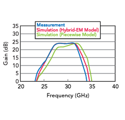
Figure 11 Measured gain vs. simulations using the hybrid EM device model and piecewise device model for the MMIC PA.
Measured versus simulated performance using the hybrid EM device model for power is shown in Figure 10. The hybrid EM device model approach achieves close agreement in power, power gain and power-added efficiency.
To compare simulation accuracy between the hybrid EM device model approach and the piecewise model design approach, Figure 11 shows the small-signal gain result from Figure 9 compared with the piecewise simulation result. The gain from the piecewise approach is shifted approximately 1 GHz higher in frequency. In addition, the gain shows an upward slope across most of the band. If the piecewise design approach was relied upon for this design, the measured result would likely have been the mirror image of this, namely the gain shifted down in frequency from the desired band by approximately 1 GHz with the gain sloped downward in frequency.
CONCLUSION
The ever-increasing demand for wireless data will continue to push wireless communication systems to higher mmWave frequencies. Designing PA MMICs for these systems will continue to be challenging as many systems will have different MMIC specifications.
Designing MMICs for multi-system specifications will require more flexible design approaches. In addition, it has never been more critical to obtain first-pass design success due to the time, resources and cost. The hybrid EM device model approach, as well as other new models and methods, will be needed to support more accurate MMIC development in the future.
References
- A. Cidronali, G. Collodi, A. Santarelli, G. Vannini and G. Manes, “Small-Signal Distributed FET Modeling Through Electromagnetic Analysis of the Extrinsic Structure,” IEEE MTT-S International Microwave Symposium Digest (Cat. No.98CH36192), Vol. 1, June 1998, pp. 287–290.
- E. Larique, S. Mons, D. Baillargeat, S. Verdeyme, M. Aubourg, R. Quere, P. Guillon, C. Zanchi and J. Sombrin, “Linear and Nonlinear FET Modeling Applying an Electromagnetic and Electrical Hybrid Software,” IEEE Transactions on Microwave Theory and Techniques, Vol. 47, No. 6, June 1999, pp. 915–918.
- D. Resca, A. Santarelli, A. Raffo, R. Cignani, G. Vannini, F. Filicori and A. Cidronali, “A Distributed Approach for Millimetre-Wave Electron Device Modelling,” European Microwave Integrated Circuits Conference, September 2006.