

Autonomous vehicles require sensors that can be relied on to provide high-resolution reconstructions of their surroundings under all-weather and light conditions. Imaging radars are positioned to meet this need.
Recent announcements from full-stack players and OEMs validate the fact that conventional radars are not suitable for higher levels of autonomy. False alarms, ghost objects and missing dimensions in conventional radars have been constant pain-points. Imaging radars are quickly evolving to demonstrate an all-weather, real-time reconstruction of the world around us at a much lower cost point. The road to fully autonomous vehicles might be long but there are no shortcuts for safety and reliability.
Higher levels of autonomy can make perfect use of a tightly knit sensor suite of camera and radar. The present generation radars are well known for lower cost with high reliability in all-weather scenarios. Imaging radars add the missing dimensions to deliver high-resolution, which sensor fusion engines can use for navigation to enable full autonomy beyond just providing warning signals.
With an operational frequency range of 76 to 81 GHz, imaging radars must resort to massive MIMO approaches to achieve an angular resolution of less than 1 degree, an order of magnitude better than conventional radars. However, merely an extension of the present-day philosophy of increasing physical arrays and using 4D FFT compute engines is hardware cost, compute and power intensive. Better system partitioning across the radar IC and antenna system aid signal processing engines to achieve high-resolution imaging radar solutions that are commercially viable and optimal for power consumption. With reliability at the heart of automotive systems, these techniques must also adhere to the safety standards of the automotive world.
CMOS RADAR
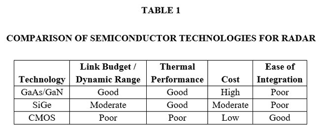
Traditionally, solid-state radars have been designed with discrete modules using GaAs/GaN and SiGe BiCMOS technologies. Owing to this, only tiny radar apertures of four to five antennas can be realized, which is hardly enough to achieve angular resolutions comparable to lidar.
Table 1 is a comparison of CMOS technology with GaAs/GaN and SiGe BiCMOS for radar applications. Due to low power gain at high frequencies and limited voltage handling capabilities, CMOS technology suffers from poor link budget margin and limited dynamic range. This shortcoming is addressed by building massive MIMO radar arrays, which in turn helps to achieve optical sensor-like angular resolution.
Along with improved IC fabrication technology, automotive radar design, due to stringent reliability requirements, must place an emphasis on packaging as well. An automotive grade package must have good mechanical reliability and thermal performance. Along with this, good mmWave electrical performance and low cost are also desirable. Traditionally, the flip chip ball grid array has been the package of choice for automotive radar ICs, however, the industry trend is toward the embedded wafer level ball grid array (eWLB) due to its cost advantage and scalable pin count. Once mechanical stability, thermal reliability and cost are addressed, careful design and modeling of signal routing from IC I/O’s to the PCB must be done to ensure good performance at mmWave frequencies.
Enhancements in frequency modulated continuous wave (FMCW) techniques through fast-chirping, high sampling data converters (> 80 MSps) and high speed data communications channels (14.4 Gbps per chip) have brought unprecedented performance to conventional radar. Linear high bandwidth FMCW enables a range resolution of sub-4 cm, which enhances the overall system point cloud density. A high dynamic range receiver chain is required for scenarios like the detection of vulnerable road users by-the-side of heavy metallic objects (like trucks, fences and grills) and urban driving. High speed interfaces enable a choice of processing architectures, such as edge versus central, for OEMs.
ANTENNA CHALLENGES
Like the radar IC, mmWave antenna design for radar is equally challenging. Key performance parameters are wide bandwidth, low side lobe levels, high gain and good radiation efficiency. For lower cost and ease of manufacturing, printed structures like microstrip or comb antennas are preferred for automotive radar. These contain resonant elements, and therefore have narrow bandwidths compared to helical or horn antennas. Wide bandwidth is desired as it is necessary for good range resolution. To achieve wide bandwidths with microstrip and comb antennas, a careful choice of substrate thickness, dielectric constant, patch impedance and routing impedances is required. For good radiation efficiency, one must choose low loss substrates.
A massive array for imaging radar requires feed lines that are several wavelengths long. This causes spurious radiation and pattern distortion, which can be comparable to the antenna’s own gain. The main issue with parasitic radiation is pattern distortion, which limits the maximum achievable angular resolution. This is addressed by careful feed line modeling and design.
Modeling Antenna Feed Lines to Avoid Spurious Radiation
Designing a MIMO antenna and feed line layout at mmWave frequencies and ensuring a high degree of isolation between different elements/parts is a challenge. At 81 GHz, feed lines can radiate as well as couple to other feed lines. Consequently, the effective radiation pattern and system efficiency degrade; in some cases, this can cause undesired nulls in the pattern and reduce the overall SNR of the radar system. Two major aspects of the design that affect radiation quality are isolation and surface wave mitigation.
Isolation between antennas and feed lines can be improved by spacing them from each other as far as possible. In practical MIMO designs this spacing is not an independent parameter but determined by spatial sampling requirements. In such scenarios, creative isolation structures can be employed. A MIMO antenna array section that uses such an isolation structure is shown in Figure 1. This scheme exploits the symmetry of coplanar waveguide (CPW) with the addition of a grounded shield to control cross talk between the feed lines and improve the radiation pattern (see Figure 2).
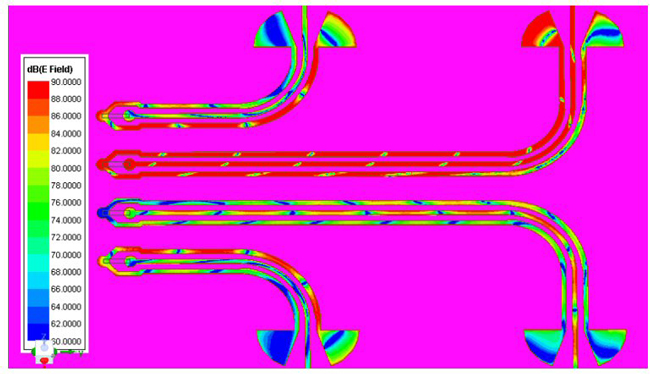
Figure 1a
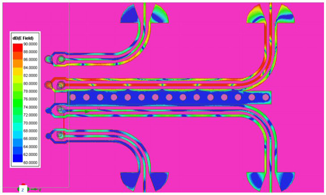
Figure 1b
Figure 1 MIMO antenna array section without isolation (a) and with isolation vias between feed lines (b).
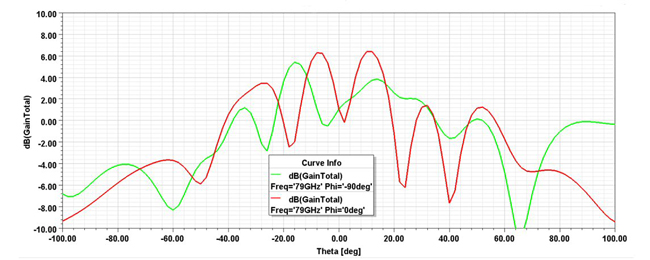
Figure 2a

Figure 2b
Figure 2 Array radiation patterns before (a) and after (b) shielding.
Surfaces waves can increase the coupling between elements of the PCB and may also result in direct spurious radiation. In the case of a MIMO antenna array, this can degrade the pattern and efficiency of the antenna. By creating an appropriate ground reference with via patterns, it is possible to control surface wave propagation to a great extent. Minimizing substrate height, bends and stubs on feed lines are other things that can be done to reduce surface wave propagation.