
Using a clipped and filtered, modulated 5G NR waveform with 7.5 dB PAR, the nominal RF operating power of 39 dBm is predicted, with the first peak in DE expected near this point, to ensure minimal deviation of the modulated DE from the single-tone DE. The single-tone DE was 52 to 54 percent. The performance of the GaN on Si PAM is comparable to the performance reported for GaN on SiC.13-15

Figure 9 Measured gain (a) and DE (b) vs. ourput power of a single-stage Doherty PA.
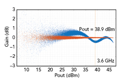
Figure 10 Gain vs. Pout of the Doherty PA with a 3.6 GHz modulated signal, comparing the “raw” performance (blue) with DPD linearization (red).
The dynamic peak power of the PAM with a modulated signal and using digital predistortion (DPD) was measured at 3.6 GHz using a spectrum analyzer (see Figure 10). A peak power of 47.5 dBm was measured. The figure compares the modulated AM-AM dependency with and without DPD, showing the DPD yields excellent linear output characteristics. The capability of DPD to linearize the PAM reflects low device nonlinearity and low circuit and device memory effects. Ease of linearization using commercially available DPD engines is an important characteristic of the device technology and amplifier design.
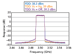
Figure 11 Measured Doherty PA spectrum in FDD and TDD modes using DPD without the long-term memory model.
The fielded application for this PAM is in FDD and TDD base stations. With the versatility of the 3GPP’s 5G standards, the time diagram of a transmitted signal can be rather complex and irregular, with single symbol transmission possible. Thermal, charge trapping and video bandwidth determine the dynamic response of the PAM, which manifests in varying output power and error vector magnitude along the symbol sequence within a transmitted sub-frame. To illustrate, Figure 11 plots the power spectrum of the first symbol of a transmitted sequence, showing performance in FDD, mixed and TDD modes using DPD without the long-term memory model. Vc refers to the clamping voltage or off-stage gate bias. The TDD mode measurements used the following modulated signal: 3GPPD TM3.1a with a 1 × 20 MHz channel, 5G NR OFDM 256-QAM, 60 kHz SCS and 7.5 dB PAR.
TRENDS AND CHALLENGES
As the RF transmit power increases, heat management becomes more important. With mMIMO AAS, there are several thermal management considerations: 1) system overheating leading to component performance degradation and reduced long-term reliability, 2) higher operating cost because of lower energy efficiency and 3) passive heat removal from the radio system.
While discrete module solutions could provide better heat management through lower packaging density, they can create BOM and PCB-area bottlenecks in larger AAS, requiring significant design optimization by the system integrator. Control over die thickness, use of proper die attach techniques and high-quality soldering of the PAM onto the PCB are key to removing heat from the PAM. Maintaining near constant output power over temperature requires a smaller design margin and yields higher PAE. Infineon’s GaN on Si PAM products have a -0.02 dB/°C power gain coefficient, which is comparable to GaN on SiC and LDMOS PAs.
Wider instantaneous bandwidth and use of frequency bands above 5 GHz are two additional market trends leading to more integrated PAM solutions on GaN. Infineon’s GaN on Si technology has the capability for MMIC integration, which offers substantial benefits, not only for meeting the output power specifications, but also overcoming performance limitations from the parasitic effects of cascading discrete components, transistor parasitics and bond wires, which typically result in reduced bandwidth and poorer energy efficiency.
SUMMARY
This article discussed the development of an RF GaN on Si technology for wireless infrastructure that improves the cost-performance value of GaN. After many years of GaN on Si development, the technology has matured to deliver its potential, providing efficiency on par with GaN on SiC at a lower cost based on Si wafer processing. This article has shown GaN on Si can meet the efficiency, linearization and power density requirements of 5G wireless communication systems. We believe this is the start of a longer journey, where further industry developments will push the capabilities of GaN on Si to higher frequencies and higher power levels, potentially expanding applications beyond wireless infrastructure.
References
- N. Jones, “How to Stop Data Centres from Gobbling Up the World’s Electricity,” Nature 561, 2018, pp. 163–166, doi.org/10.1038/d41586-018-06610-y.
- 3GPP, Release 16, www.3gpp.org/release-16.
- “5G Power White Paper,” Huawei Technologies Co. Ltd., https://carrier.huawei.com/~/media/CNBG/Downloads/Spotlight/5g/5G-Power-White-Paper-en.pdf.
- Y. Tarui, Y. Hayashi and T. Sekigawa, “Diffusion Selfaligned MOST; A New Approach for High Speed Device (1.Electrotechnical Lab.)” https://doi.org/10.7567/SSDM.1969.4–1.
- A. Wood, C. Dragon and W. Burger, “High Performance Silicon LDMOS Technology for 2 GHz RF Power Amplifier Applications,” IEEE International Electron Devices Meeting (IEDM), 1996, pp. 87–90.
- H. F. F. Jos, “Novel LDMOS Structure for 2 GHz High Power Basestation Application,” European Microwave Conference, 1998, pp. 739–744.
- M. Rosker, “The Wide and the Narrow: DARPA/MTO Programs for RF Applications in Wide Bandgap and Antimonide-based Semiconductors,” IEEE Compound Semiconductor Integrated Circuit Symposium, 2005, pp. 4, https://doi.org/10.1109/CSICS.2005.1531739.
- “Wide Band Gap Semiconductors for RF Applications,” Federal Grants, https://www.federalgrants.com/Wide-Band-Gap-Semiconductors-for-RF-Applications-WBGS-RF-1240.html.
- E. Cohen, “The MIMIC Program - A Retrospective,” Microwave Magazine, June 2012, pp. 77–88. https://doi.org/10.1109/MMM.2012.2189989.
- B. Green, K. Moore, D. Hill, M. CdeBaca and J. Schultz, “GaN RF Device Technology and Applications, Present and Future,” IEEE Bipolar/BiCMOS Circuits and Technology Meeting (BCTM), 2013, pp. 101–106, https://ieeexplore.ieee.org/document/6798154.
- H. Wang, T.-Y. Huang, N. S. Mannem, J.Lee, E. Garay, D. Munzer, Ed. Liu, Y. Liu, B. Lin, M. Eleraky, H. Jalili, J. Park, S. Li, F. Wang, A. S. Ahmed, C. Snyder, S. Lee, H. T. Nguyen and M. E. Duffy Smith, “Power Amplifiers Performance Survey 2000-Present,” Georgia Tech Electronics and Micro-System Lab (GEMS), https://gems.ece.gatech.edu/PA_survey.html.
- T. Detzel, A. Charles, G. Deboy, O. Haeberlen and T. McDonald, “The Commercialization of GaN Power Devices: Value Proposition, Manufacturing, and Reliability,” Compound Semiconductor Week (CSW), 2019, pp. 1–1, https://ieeexplore.ieee.org/document/8819303.
- S. Sakata et al., “A Fully-Integrated GaN Doherty Power Amplifier Module with a Compact Frequency-Dependent Compensation Circuit for 5G massive MIMO Base Stations,” IEEE/MTT-S International Microwave Symposium (IMS), 2020, pp. 711–714, https://ieeexplore.ieee.org/document/9223897.
- K. Moore et al., “High Performance 150 mm RF GaN Technology with Low Memory Effects,” 2020 IEEE BiCMOS and Compound Semiconductor Integrated Circuits and Technology Symposium (BCICTS), 2020, pp. 1–4, https://ieeexplore.ieee.org/document/9392951.
- P. Saad, R. Hou, R. Hellberg and B. Berglund, “An 80 W Power Amplifier with 50% Efficiency at 8 dB Power Back-off over 2.6-3.8 GHz,” 2019 IEEE MTT-S International Microwave Symposium (IMS), 2019, pp. 1328-1330, https://ieeexplore.ieee.org/document/8701113.