
A novel dual-bias circuit structure increases a power amplifier’s video bandwidth while reducing the memory effect, thereby improving its linearity. A Doherty power amplifier (DPA) operating in the 5G communication band (3.4 to 3.6 GHz) and incorporating this circuit achieves a saturated output power of 43 to 44 dBm with a saturated drain efficiency greater than 70 percent. Drain efficiency is 51 to 55 percent at 6 dB power back-off and greater than 43 percent at 8 dB back-off. As output power reaches 42.7 dBm, the adjacent channel leakage ratio (ACLR) is less than -46 dBc combined with digital predistortion (DPD).
For increasing the data transmission rate and the capacity of wireless communication systems, modulation signals with high peak-to-average power ratios (PAPR) are widely applied, and DPAs have become the mainstream for base station power amplifiers.1-4 Correspondingly, video bandwidth (VBW) and memory effect are two important factors in Doherty RF power amplifier performance.5
VBW plays a significant role in the operating bandwidth of the PA and affects the degree of DPD correction.6 If the instantaneous signal bandwidth is very close to the VBW, PA linearity is seriously deteriorated and is difficult to correct with DPD.7,8 It can also cause large voltage and current offsets in the active device, resulting in high internal temperatures and component damage.
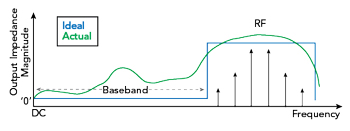
Figure 1 Ideal vs. actual RF impedance.
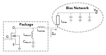
Figure 2 Typical transistor bias circuit.
Several methods to decrease the memory effect and enlarge VBW have been proposed.9,10 Ladhani et al.9 obtained wider VBW by directly connecting series resonant circuits to the gate and drain electrodes of a transistor die in a package. This method is based on the design of the transistor current plane and is not suitable for practical circuit design. In addition, an LC resonant bias network has been proposed to diminish baseband impedance for reducing the electrical memory effect;10 however, the harmful effect of this method is that the fundamental impedance decreases while reducing the baseband impedance. The smaller fundamental impedance causes RF power to leak into the bias circuit. Furthermore, lumped-parameter components with large parasitic elements are difficult to use in RF circuits.
This article describes a high efficiency and high linearity 3.4 to 3.6 GHz DPA with a novel dual-bias network structure to broaden the VBW and minimize memory effects in a wideband DPA when transmitting a 20 MHz A-LTE modulation signal. With the addition of linearization technology, this DPA exhibits good linearity and high efficiency.11-16
KEY TECHNOLOGIES
Memory Effect
In a field-effect transistor amplifier, the majority of undesirable memory effects are attributed to the baseband impedance, and the baseband impedance is mainly determined by the impedance of the bias network in the low frequency band.17,18 When employing DPD in an RF PA it is particularly important to reduce the memory effect. The baseband impedance, Z, should be short-circuited at low frequencies (see Figure 1); but unfortunately, it is not. The presence of baseband impedance causes the voltage at the drain of the power transistor to change with input signal level. To reduce memory effect, the baseband impedance of the drain bias must be minimized.
VBW
In modern communication systems, wide bandwidth and multi-carrier modulation have been used for high speed data transmission. Nevertheless, the modulation signal bandwidth is limited by RFPA VBW. VBW depends mainly on the equivalent LC resonance of bias networks and transistor internal matching. Figure 2 is the equivalent circuit model of a transistor and a typical bias circuit. The equivalent resonant frequency can be expressed as:
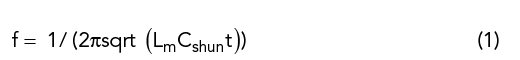
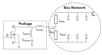
Figure 3 The dual bias circuit increases the equivalent LC resonant frequency.
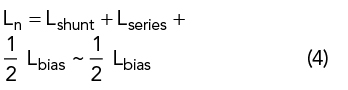
Where, Lm is the typical bias circuit equivalent inductance and Lm = Lshunt + Lseries + Lbias. Cshunt represents the shunted equivalent transistor package capacitance.
In general, Lbias is higher than Lshunt and Lseries by more than two orders of magnitude. So, Lm ≈ Lbias. Therefore, widening of the VBW can be achieved by reducing the equivalent inductance of the bias circuit.
Dual-Bias Network
Optimizing the memory effect requires reducing the baseband impedance, and increasing the VBW requires increasing the equivalent LC resonant frequency. A novel dual-bias network that does this is shown in Figure 3. Compared with a typical bias circuit, the dual-bias network is simply two bias circuits in parallel. From the principle of parallel circuits:

Where Zb1 and Zb2 are the drain bias impedances in Figures 2 and 3, respectively. Because the drain node impedance of the dual-bias network is half that of the typical bias circuit, baseband impedance is reduced and the memory effect improved.
Lbias and Lbias‘ in Figure 3 are λ/4 microstrip lines with equivalent parallel inductance of 1/2 Lbias. The equivalent resonant frequency is:
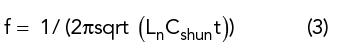
where, Ln is the dual-bias circuit equivalent inductance and Ln = Lshunt + Lseries + ½ Lbias.
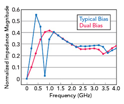
Figure 4 Simulated impedance vs. frequency of the typical and dual bias circuits.
The Cree CGH40010F transistor is used as an example. At a center frequency of 3.5 GHz, the transistor equivalent model is analyzed and the λ/4 microstrip lines equivalent inductance is calculated. Lshunt and Lseries are lower than Lbias by an order of magnitude; therefore, Ln can be expressed as:
Advanced Design System (ADS) is used to simulate the two bias circuits. The results plotted in Figure 4, show the resonant frequency of the dual-bias network to be about 1 GHz, more than twice the resonant frequency of a typical single bias network, which increases the VBW while reducing the baseband impedance.