
Two multi-modulus programmable frequency dividers (MMPFDs) with improved performance consist of eight stages of emitter-coupled logic (ECL) dual-modulus prescalers (divide by 2/3 cell). One prescaler is constructed with four master-slave D flip-flops (MS-DFFs) and three OR gates, another uses two MS-DFFs and one XOR gate. To further increase the operating frequency while reducing power consumption, the MS-DFF is modified: the hold circuits and sample circuits are controlled by the same input clock signal so that a single power supply can be used, reducing power consumption. Two frequency divider prototypes were built in 2 μm GaAs HBT technology for verification. Measured results show that the two frequency dividers can operate over a very wide frequency range - 50 MHz to 5 GHz and 50 MHz to 8 GHz, respectively - and their division ratios are 256 to 511 with a unit step increment.
Frequency dividers are key components of phase-locked loop (PLL) frequency synthesizers, which are widely used in modern communication and radar systems. High performance frequency dividers with wide operational frequency bandwidths, low-power consumption, wide division ratios and low phase noise are in demand. Various frequency divider topologies have been studied and built using compound semiconductor processes (InGaP, GaAs or GaN) and Si bulk (CMOS or BiCMOS) in recent years.1-10
Most employ Si bulk technology because dividers using this technology are easy to be implemented and have lower power consumption. However, relatively high substrate losses resulting in low-quality factors and noise, such as low frequency flicker noise, restricts use of silicon in applications with demanding high frequency performance requirements. For these applications, compound semiconductors such as InGaP, GaAs and GaN are attractive alternatives; however, MMPFD based on compound semiconductor processes remain difficult to implement due to high-power consumption and the large amount of circuit area required.
Synchronous current mode logic (CML) or ECL architectures are the most popular because of a wide operational frequency range.1-6 Li et al.1 describe a 5.5 GHz pulse-swallowing multi-modulus frequency divider with divide ratios from 256 to 511. It is composed of a CML divide by 4/5 prescaler and a digital programmable arbitrary modulus counter. Wang et al.4 describe a multi-modulus frequency divider using cascaded divide by 2/3 cells. The divide by 2/3 cell consists of four ECL D-latch and three AND gates; however, the fabrication processes are either Si bipolar or CMOS. In recent years, several dividers using compound semiconductor processes have been reported.7-10 Tseng et al.7 describe a divide by 3 prescaler using GaInP/GaAs HBT technology. Shin, Won et al.8, 9 describe a semi-dynamic frequency divider with a division ratio of 1.5. In addition, Osafune and Ohwada10 report on a GaAs MESFET frequency divider. The division ratios of these dividers, however, are limited and cannot be changed. It remains a challenge to design a compound semiconductor frequency divider with a wide division ratio that does not consume high DC power.
In this work, two MMPFDs were designed and implemented using a 2 μm GaAs HBTs process technology. Simulation shows a power reduction of more than 180 and 240 percent, respectively, compared to reported traditional dual-modulus divide by 2/3 prescalers. A considerable decrease in die area was also achieved. To our knowledge, these are the first reported MMPFDs with such a wide operational frequency range and range of division ratios using GaAs HBT technology.
DESIGN
Previous 2/3 Divider Cell
A popular method for PLL realization is hybrid integration, in which the voltage-controlled oscillator is implemented by a compound semiconductor process and the other circuits - the frequency divider and phase frequency detector - are implemented in silicon (CMOS or SiGe). For a fully integrated PLL, nearly all are realized in silicon. Silicon-based frequency dividers are easily fabricated using available foundries and can be integrated with high speed digital and mixed-signal circuits to facilitate system interface designs. Thus, academic and industrial applications are more inclined to use silicon dividers for on-chip system compatibility, ease of integration and low-power consumption; however, the multi-modulus frequency divider still remains difficult to integrate in the same process, since area overhead and power consumption is huge.
In summary, the main difficulties designing MMPFDs using compound semiconductor processes (GaAs, InP and GaN) are:
- The focus of academia and industry has been on the analysis and optimization of CMOS frequency dividers; however, some of the theoretical analysis and structures are not always available in compound semiconductor design
- For the programmable frequency divider, the larger division ratio means more dual-modulus divider cells, yielding a larger die area and higher power consumption
- The relatively crude process design kit and immature electronic design automation prevent academic researchers from gaining deep insight into the compound semiconductor frequency divider
- With traditional design methods, the frequency divider based on compound semiconductor processes faces difficult problems, such as large chip area, high-power consumption and high design complexity.
A variety of structures and methods have been proposed to realize the 2/3 divider cell, including a commonly used structure1-5 containing four D-latches and three AND gates (see Figure 1). However, these logic circuits AND gates increase propagation delay, resulting in a lower operating frequency. Also, the latch output is not stable. During the update phase, any input change will be passed to the output, and the transition of the latch output is not synchronized to the edge. The 2/3 divider cell divides the input frequency by 2 or 3 as determined by the control inputs to Modin and PB. The output frequency is half of the input frequency except when Modin = 0 and PB = 0; then, the output frequency is 1/3 the input frequency. Because of the power consumption and die area for a traditional 2/3 divider cell, it is not suitable for a multi-modulus programmable frequency divider with a wide range of division ratios.
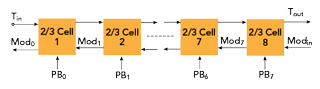
Figure 1 Conventional 2/3 divider cell.
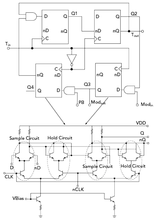
Figure 2 MMPFD structure comprising eight stages of dual-modulus, divide by 2/3 prescalers.
2/3 Divider Cell with MS-DFF and Gate (MMPFD-1)
To realize a multi-modulus programmable frequency divider for high frequencies with large division ratios and relatively low-power consumption, some improvements are needed in the structures of the dual-modulus prescaler (i.e., the 2/3 divider cell) and MS-DFF. Figure 2 shows the elementary structure of a frequency divider that consists of eight stages of dual-modulus divide by 2/3 prescalers. The 2/3 divider cell comprises four MS-DFFs and three OR gates (see Figure 3a). The D flip-flops use synchronous ECL D-latches due to their high operating frequencies. In contrast with traditional structures,1-4 the propagation delay is reduced to yield a higher operating frequency and lower power consumption.
The 2/3 divider cell divides the input frequency by 2 or 3, determined by control inputs Modin and PB. When PB = 1, Modin = 1 or PB = 0, Modin = 1 or PB = 1, Modin = 0, the 2/3 divider cell works as a divide by 2 cell. Its simplified circuit configuration and state diagram are shown in Figure 3b. When PB = 0, Modin = 0, the 2/3 divider cell works as a divide by 3 cell. Its simplified circuit configuration and state diagram are shown in Figure 3c. The division ratio of this multi-modulus frequency divider is expressed in Equation 1:
where Tout and Tin represent the output and input periods, respectively, and PB0, PB1, … PBn-2, PBn-1 represent the control bits of the MMPFD given to the cells, as shown in Figure 1.
To overcome latch output instability, a MS configuration cascades two latches. Recalling the traditional MS flip-flop shown in Figure 1, it has 14 transistors including two extra transistors used as two tail current sources. As shown in Figure 4, the sample and hold circuits of the MS-DFF are controlled by the same input clock signal, theoretically reducing power consumption by 50 percent. The structure also enables a more compact die area.
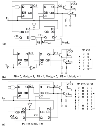
Figure 3 MMPFD-1 2/3 divider cell (a) and simplified configuration and state diagram when set to divide by 2 (b) or divide by 3 (c).
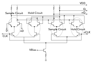
Figure 4 Sample and hold circuits of the MS-DFF.