
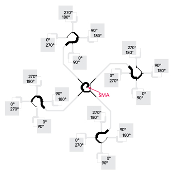
Figure 1 4 × 4 microstrip antenna array with double sequential feed network, showing relative phases for achieving circular polarization and sequential dividers shaded black.
A 4 × 4 microstrip patch antenna array with a uniplanar structure fed by a double sequential rotation feeding network was designed to provide circular polarization. Sequential dividers in the centrally branched feeding network enable the required phase shifts between the adjacent array elements, while the specific array geometry ensures a high degree of central symmetry and contributes to achieving low axial ratios. Measured results were in good agreement with the simulation. |S11| was better than -10 dB over a 13.5 percent bandwidth, gain at the center frequency of 10 GHz was around 16 dBi and the axial ratio was less than 3 dB over a 12 percent bandwidth.
Antenna arrays with circular polarization (CP) require amplitude balanced signals with precise phase shifts between the feed points of adjacent radiating elements.1 Feed networks (FNs) for such arrays may become very complex, especially with large numbers of array elements. This complexity causes degradation of FN symmetry, resulting in narrower CP bandwidth. One approach to help overcome this problem and minimize FN loss is a multilayer FN configuration.2 This, however, may introduce fabrication difficulties and increase array volume, weight and cost. Microstrip antenna arrays without multilayer feeding structures are usually realized with at most 2 × 2 radiating elements, achieving gains around 13 dBi.3-5
The chosen method of generating CP in patch radiating elements affects the antenna structure complexity and electrical and radiation characteristics as well. CP is achieved by exciting two orthogonal modes, either by using dual feeds or a single feed and a perturbed patch structure. The single feed technique is simple and compact but provides very narrow impedance and axial ratio (AR) bandwidths, where the AR bandwidth is typically a fraction of the impedance bandwidth. By increasing the number of radiating elements in the array and applying a carefully designed FN that compensates for amplitude imbalances and phase errors, the characteristics of the array can be significantly improved.6 Configurations with parasitically coupled stacked patches are often used to overcome these disadvantages.7,8 While they provide higher gain, they are more complicated to fabricate.
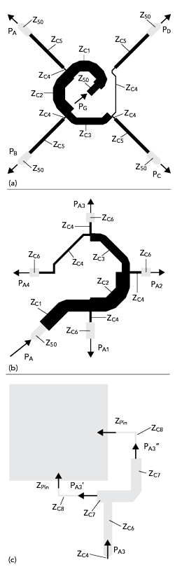
Figure 2 Central sequential divider (a), peripheral sequential divider (b) and radiating element with feed network (c).
A dual-feed configuration is the most direct way of exciting two orthogonal modes of equal amplitudes and 90-degree phase difference, by introducing a 90-degree phase shift in one of the two feed lines. Shifting the impedance from one input through a quarter-wavelength line before combining the two lines in parallel cancels some reflection from the second line and increases the impedance bandwidth.9 The impedance bandwidth is approximately twice as wide as the bandwidth of a single-fed patch, and the AR bandwidth is comparable to the impedance bandwidth.10
This work introduces a 4 × 4 uniplanar microstrip antenna array with a double sequential FN, fulfilling the conditions for obtaining CP as well as achieving higher gain. The high degree of central symmetry helps maintain low AR values over a wider range of frequencies. As both the antenna array and feed network are fabricated on the same dielectric substrate using standard photolithography, the design is highly reproducible using low-cost production techniques.
SEQUENTIAL FEEDING NETWORK DESIGN
The main feed point of the FN is in the symmetrical center of the antenna structure through an SMA connector soldered perpendicular to the ground plane (see Figure 1). The main part of the FN is a sequential divider (see Figure 2a) composed of λ/4 transformers with characteristic impedances optimized to obtain signals with equal amplitudes at all its outputs and π/2 phase differences between the adjacent ports. The input signal PG is divided into four signals, PA, PB, PC and PD, with relative phases θPA = 0, θPB = 90, θPC = 180 and θPD = 270 degrees. One of the possible sets of characteristic impedances that obtain signals with these characteristics is: ZC1 = 35.35, ZC2 = 33.33, ZC3 = 50 and ZC4 =100 Ω, while the electrical lengths of the strips with impedances ZC1, ZC2, ZC3 and the long segment of the strip with ZC4 are π/2 at the central frequency of 10 GHz. The 100 Ω output lines of the sequential divider are matched to the 50 Ω microstrip lines using λ/4 transformers with ZC5 = 70.7 Ω.
The peripheral sequential dividers (see Figure 2b) serve the same purpose as the central one, so their structures are almost identical, differing only in form: the λ/4 input transformers with ZC1 are bent away from the sequential divider and toward the 50 Ω microstrip lines that connect the peripheral sequential dividers with the central one. As indicated in Figure 2b, one of the signals (PA) coming from the output port A of the central divider is split into four signals, PA1, PA2, PA3 and PA4, having equal amplitudes and a successive phase difference of π/2 between adjacent ports.
At the outputs of a peripheral sequential divider are short segments of microstrip line with characteristic impedance ZC4 = 100 Ω, matched to the radiating element feed circuits with the λ/4 transformer ZC6. The feeding sub-network of the array radiating elements (see Figure 2c) is used for matching the input impedances of the square-shaped microstrip patches (180 to 220 Ω, depending on the thickness of the dielectric substrate) to the output impedance of the peripheral sequential divider, ZC4, selected to be 100 Ω.
The input impedances of the patches with the λ/4 transformers (ZC8 = 70 to 100 Ω), are matched to ZC7 (30 to 50 Ω). The phase difference between the electrical length of the short and long segments of the microstrip line with ZC7 equals π/2 at the center frequency of 10 GHz. The λ/4 transformer with ZC6 (40 to 50 Ω) at the input of the radiating element matches the impedance ZC7/2 to the output impedances of the peripheral sequential dividers ZC4. By combining phase differences provided by the central and peripheral sequential dividers, as well as the FNs of the patches, the input signal PG is divided into 32 signals of equal amplitude and relative phases as indicated in Figure 1. The antenna array has a low AR with this condition maintained, which solely depends on the structure and characteristics of the overall FN. The exact relative phases shown in Figure 1 are achieved at a single frequency, aligned with the lowest resonant frequency of the square patch, where the patch has the best radiating efficiency.
REALIZATION AND MEASURED RESULTS
The antenna array was fabricated on a 0.254 mm thick Teflon-fiberglass dielectric substrate with εr = 2.17, tanδ = 0.0009 and metallization thickness t = 0.017 mm. The square-shaped patches with side lengths of 9.9 mm were spaced 0.88 λ apart (26.55 mm) in both directions and inclined by 30 degrees with respect to the horizontal and vertical axes (see Figure 3).
An SMA connector was mounted on the backside of the antenna array and its central pin was connected to the input port of the central sequential network, while the outer conductor was soldered to the reference ground plane of the microstrip substrate (see Figure 4a). As shown in Figure 3, both left-hand CP (LHCP) and right-hand CP (RHCP) versions were built, two of each for determining antenna gain based on the measurement of free-space loss between two identical antennas.