
SIMULATED VERSUS MEASURED RESULTS
Several sets of measurements were made at Michigan State University (MSU), the University of Massachusetts (UMass) Amherst and the National Institute of Standards and Technology (NIST). The 20 to 28 and 35 to 41 GHz filters were tested at MSU and at NIST, while the 40 to 56 GHz filter was measured at UMass. The tests at NIST verified performance repeatability for two sets of the same filters and identified any response variations under different power levels at 0 and -10 dBm.1 They were performed with vector network analyzers (VNA) equipped with ground-signal-ground probes; 150 μm pitch probes for the 40 to 56 GHz filter and 250 μm pitch probes for the 20 to 28 and 35 to 41 GHz designs. The reference plane was at the filter feed point.
For the probe measurements at UMass and MSU, short-open-load-thru calibrations used a commercial substrate. At NIST, on-wafer calibration artifacts fabricated on a sapphire substrate were used to correct the filter S-parameters. The calibration artifacts include a 0.420 mm thru, a short circuit reflection, a nominal 50 series resistor, a series capacitor and a series of transmission lines. The short circuit reflection, series resistor and series capacitor had 0.210 ±0.005 mm offsets. In cross section, each device has a CPW geometry, where the center conductor is 0.060 ±0.001 mm, the ground planes are 0.240 ±0.001 mm and the gaps are 0.015 ±0.001 mm. Conductor thicknesses are nominally 0.350 ± 0.010 nm. Transmission lines lengths of 0.420, 1.000, 2.155, 3.135, 4.200, 7.615 and 11.570 mm were optimally chosen to reduce measurement uncertainty. An uncertainty of 0.005 mm was due to probe contact variability.
To correct the on-wafer test data, S-parameters of each calibration artifact and the switch terms were measured with a VNA. First, data for the switch terms was corrected, reducing the error model from twelve to eight terms.17 Next, a multiline thru-reflect-line (TRL) calibration,18, 19 was performed, with capacitance per unit length extracted from the series resistor.20 Taking the capacitance per unit length as constant, the characteristic impedance was transformed to 50 , and the reference planes translated to the probe tips.21 Finally, the filter S-parameters were measured and corrected using the multiline TRL algorithm.
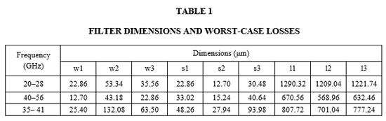
The response of the 20 to 28 GHz filter is shown in Figure 6. The magnitude of the filter’s scattering parameters, S11 and S21 in dB, and the group delay are plotted versus frequency. The vertical green lines define the desired passband, which shows a measured insertion loss of less than 2 dB and |S11| better than 17 dB. Figure 6b shows excellent agreement between the simulated results and two experimental datasets recorded using different setups by different groups. Figure 6d clearly shows the guard band helps keep group delay ripple outside the 20 to 28 GHz range. The nearly constant 0.2 ns group delay in the passband introduces minimal phase distortion in the chirp signal.
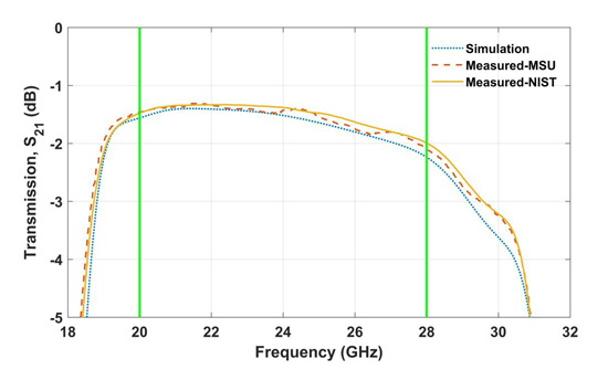
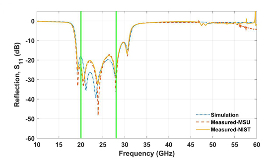
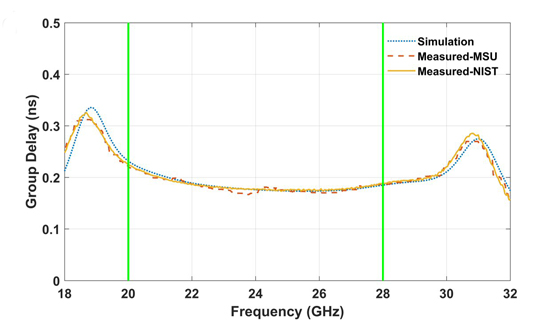
Figure 6 Simulated vs. measured responses of the 20 to 28 GHz filter: transmission magnitude (a), zoomed-in view of the passband (b), reflection magnitude (c) and group delay (d).
Figure 7 shows the response of the 40 to 56 GHz filter, demonstrating an insertion loss of less than 2.5 dB, including the effect of the CPW to microstrip transition and the ribbon bonds used in the test setup. Figure 8 shows the filter and CPW transition interconnect with two gold ribbon bonds. The use of multiple parallel ribbons reduces inductance and eliminates the need to model this feature in the simulations.22 As observed in Figure 7, even with the effect of the ribbon interconnects, the filter’s measured insertion loss is lower than designs operating at similar frequencies reported in the literature.23-25 The |S11| is higher than 12 dB in the passband. Rejection at the upper end of the band is measured to only 67 GHz, due to limitations in the test setup; however, it is apparent that out-of-band signals are sufficiently attenuated and agreeing with simulation. Because of the higher operating frequencies, this design is more susceptible to fabrication inaccuracies. Figure 7b shows the measured passband is slightly wider than predicted by the simulation, which is attributed to slight differences in the dimensions of the fabricated circuit. However, the sensitivity analysis helps identify these potential discrepancies and determines the required band offsets to compensate.
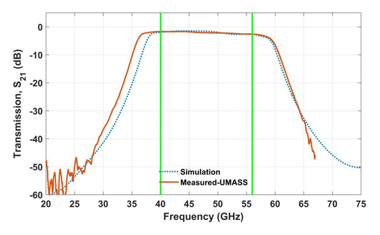
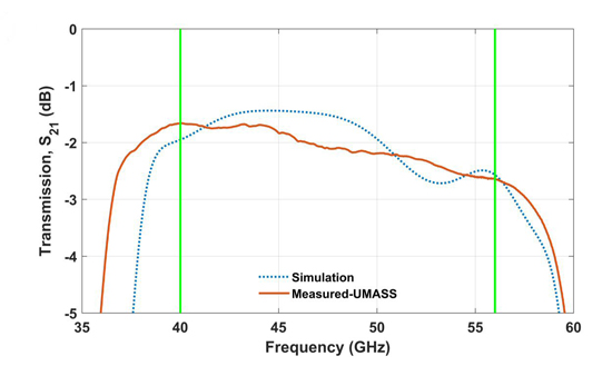
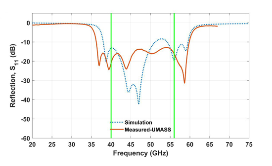
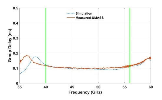
Figure 7 Simulated vs. measured responses of the 40 to 56 GHz filter: transmission magnitude (a), zoomed-in view of the passband (b), reflection magnitude (c) and group delay (d).
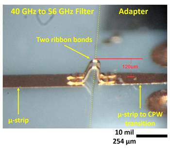
Figure 8 Ribbon bonds connecting the microstrip feed of the 40 to 56 GHz filter and microstrip to CPW adapter.
Figure 9 compares the measured and simulated responses for the 35 to 41 GHz filter. The red line indicates the 38 GHz frequency of the LO shown in Figure 1, for which the filter has less than 2 dB insertion loss and about 15 dB |S11|. Once again, both measured data sets agree well with one another and with the simulated results.
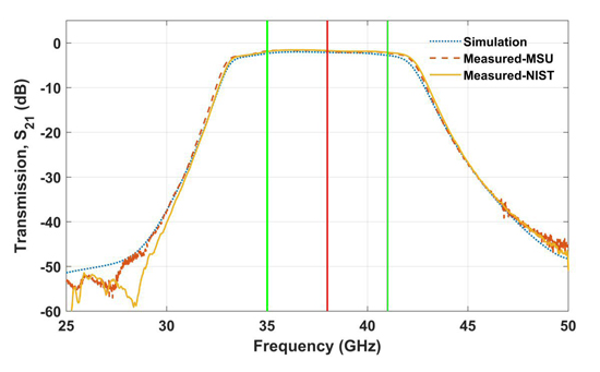
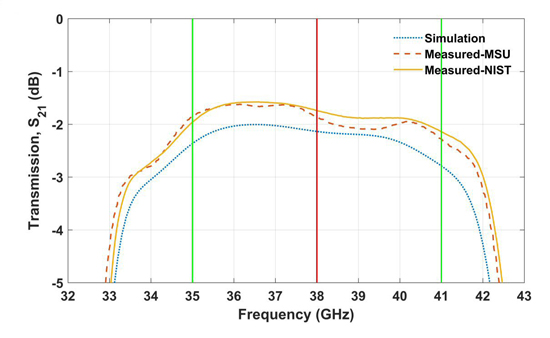
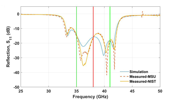
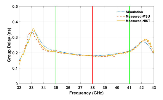
Figure 9 Simulated vs. measured responses of the 35 to 41 GHz filter: transmission magnitude (a), zoomed-in view of the passband (b), reflection magnitude (c) and (d) group delay.
CONCLUSION
Filters on ceramic substrates operating to 56 GHz exhibit greater than 33 percent fractional bandwidth. First-pass design success is accomplished on multiple prototypes by using electromagnetic simulations and performing sensitivity analyses to account for fabrication tolerances in commercial foundry processes. Measured performance is reproducible in different laboratories and is in close agreement with simulation. The filters can be easily integrated into the frequency multiplier module for which they were designed. The procedure used for development is repeatable, efficient, cost-effective and suitable for future designs operating at other frequencies.
ACKNOWLEDGMENTS
This work was completed with support from NASA (grant NNX13AQ30A) and NSF (NSF-0424589). Drs. J. Bardin and J. Papapolymerou are gratefully acknowledged for facilitating access to the probe stations at their respective institutions. We would like to thank R. Miller from UltraSource for his valuable input during the fabrication process and D. Trawczynski from Hesse Mechatronics for working on the ribbon interconnects used to test the 40 to 56 GHz prototype. Certain commercial equipment, instruments or materials are identified in this paper to specify the experimental procedure adequately. Such identification is not intended to imply recommendation or endorsement by the National Institute of Standards and Technology, nor is it intended to imply that the materials or equipment identified are necessarily the best available for the purpose.
REFERENCES
- D. S. Jun, D. Y. Lee, D. -Y. Kim, S. S. Lee and E. S. Nam, “A Narrow Bandwidth Band-Pass Filter with Symmetrical Frequency Characteristics,” ETRI Journal, Vol. 27, No. 5, October 2005, pp. 643-646.
- C. -L. Huang, J. -J. Wang and Y. -P. Chang, “Using High Permittivity Ceramic Substrates to Design a Bandpass Filter With Open Stub,” Microwave and Optical Technology Letters, Vol. 49, No. 4, April 2007, pp. 771-773.
- D. Maassen, F. Rautschke and G. Boeck, “Design and Comparison of Various Coupled Line Tx-Filters for a Ku-Band Block Upconverter,” German Microwave Conference (GeMiC),March 2016.
- M. A. Abdalla and A. A. Ibrahim, “Metamaterials Sculpt UWB Bandpass Filter,” Microwaves and RF, March 2017. Web. http://www.mwrf.com/passive-components/metamaterials-sculpt-uwb-bandpass-filter.
- K. Singh and K. Nagachenchaiah, “Compact Ultra-Wideband Microstrip Bandpass Filter Using SIR Approach,” High Frequency Electronics, Vol. 8, No. 7, July 2009, pp. 46-49.
- Z. Zhang, J. -Z. Gu, C. Wang and X. -W. Sun, “Millimeter Wave Bandpass Filter Using Three-Line Microstrip Structures,” Microwave and Optical Technology Letters, Vol. 49, No. 1, January 2007, pp. 40-42.
- F. Iturbide-Sanchez, Design, Fabrication and Deployment of a Miniaturized Spectrometer Radiometer Based on MMIC Technology for Tropospheric Water Vapor Profiling, Ph.D. dissertation, Electrical and Computer Engineering, University of Massachusetts, 2007.
- P. Ferrand, D. Baillargeat and S. Verdeyme, “Innovative Technologies for Quasiplanar Millimeter Wave Filtering Applications,” International Journal of RF and Microwave Computer-Aided Engineering, Vol. 17, No. 1, January 2007, pp. 96-103.
- F. Sabath, E. L. Mokole and S. N. Samaddar, “Definition and Classification of Ultra-Wideband Signals and Devices,” URSI Radio Science Bulletin, Vol. 2005, No. 313, June 2005, pp. 12-26.
- H. M. Talasila, Modular Frequency Multiplier and Filters for the NASA Global Hawk Snow Radar, M.S thesis, Electrical Engineering and Computer Science, University of Kansas, 2017.
- D. G. Kocher, "Digital Wideband Linear-FM Chirp Generator," MIT Lincoln Lab. Technical Report 1157, December 2010.
- Q. Li, D. Yang, X. Mu and Q. Huo, "Design of the L-Band Wideband LFM Signal Generator Based on DDS and Frequency Multiplication,” International Conference on Microwave and Millimeter Wave Technology (ICMMT), May 2012.
- D. Gomez-Garcia, C. Leuschen, F. Rodriguez-Morales, J. -B. Yan and P. Gogineni, “Linear Chirp Generator Based on Direct Digital Synthesis and Frequency Multiplication for Airborne FMCW Snow Probing Radar,” IEEE MTT-S International Microwave Symposium, June 2014.
- J. B. Yan, D. Gomez-Garcia, J. W. McDaniel, Y. Li, P. Gogineni, F. Rodriguez-Morales, J. Brozena and C. Leuschen, Ultrawideband FMCW Radar for Airborne Measurements of Snow Over Sea Ice and Land, IEEE Transactions on Geoscience and Remote Sensing, Vol. 55, No. 2, February 2017, pp. 834-843.
- G. Matthaei, E. M. T. Jones and L. Young, Microwave Filters Impedance-Matching Networks and Coupling Structures, McGraw-Hill, Inc., 1964.
- R. Miller, UltraSource, Inc, Private communication, 2016.
- R. B. Marks, “Formulations of the Basic Vector Network Analyzer Error Model Including Switch-Terms,” 50th ARFTG Conference Digest,December 2007, pp. 115-126.
- R. B. Marks, “A Multiline Method of Network Analyzer Calibration,” IEEE Transactions on Microwave Theory and Techniques, Vol. 39, No. 7, July 1991, pp. 1205-1215.
- D. F. Williams, J. C. M. Wang and U. Arz, “An Optimal Vector-Network-Analyzer Calibration Algorithm,” IEEE Transactions on Microwave Theory and Techniques, Vol. 51, No. 12, December 2003, pp. 2391-2401.
- N. D. Orloff, J. Mateu, A. Lewandowski, E. Rocas, J. King, D. Gu, X. Lu, C. Collado, I. Takeuchi and J. C. Booth, “A Compact Variable-Temperature Broadband Series-Resistor Calibration,” IEEE Transactions on Microwave Theory and Techniques, Vol. 59, No. 1, January 2011, pp. 188-195.
- D. F. Williams and R. B. Marks, “Transmission Line Capacitance Measurement,” IEEE Microwave and Guided Wave Letters, Vol. 1, No. 9, September 1991, pp. 243-245.
- M. A. Morgan, Millimeter-Wave MMICs and Applications, Ph.D. dissertation, Engineering and Applied Science, California Institute of Technology, 2003.
- Y. Amano, A. Yamada, E. Suematsu and H. Sato, “A Low Cost Planar Filter for 60 GHz Applications,” Microwave Journal, March 2001. Web. http://www.microwavejournal.com/articles/3164-a-low-cost-planar-filter-for-60-ghz-applications.
- M. Ito, K. Maruhashi, K. Ikuina, T. Hashiguchi, S. Iwanaga and K. Ohata, “A 60-GHz-Band Planar Dielectric Waveguide Filter for Flip-Chip Modules, IEEE Transactions on Microwave Theory and Techniques, Vol. 49, No. 12, December 2001, pp. 2431-2436.
- K. K. Samanta and I. D. Robertson, “An Embedded 60-GHz Planar Bandpass Filter in Multilayer Advanced Thick-Film System-In-Package Technology,” Microwave and Optical Technology Letters, Vol. 53, No. 10, October 2011, pp. 2221-2224.