
DPA Tuning
To optimize the performance of the DPA, the design needs to be tuned, paying attention to the following:
- The peaking leg in the off state may load the carrier output through the Doherty combiner, shifting it from the Zmod target impedance. The designer needs to adjust the line length of the peaking output to present a high impedance at the combining node.
- It is much easier to tune the Doherty if the test fixture design includes provisions for separately tuning the carrier and peaking outputs to each of the target impedances.
- On combination of the carrier and peaking paths, adjust the phasing between the two paths to align constructive combination.
- Tuning requires at least a couple of iterations of fine adjustments of the output matching network, input matching network, phase alignment and the bias for optimal performance.
- If the solution falls short of expectations after several iterations of fine tuning, revisit the Doherty combiner design to see if that is limiting the performance.
ISBW
The large-ISBW of a PA is usually limited by either the video bandwidth (VBW) or the RF bandwidth of the DPA circuit. VBW is usually dominated by the drain capacitance (Cds), bond wires, leadframe inductance and package parasitics, which the designer should minimize. To extend ISBW, the A3I35D025WN has special purpose pins labelled “VBW” that provide access to an internal RF “cold node” on the drain of each final stage transistor. A high-quality chip capacitor on each VBW pin provides an alternate path to RF ground for the baseband currents, avoiding inductance in the prematch network or on the drain bias feed lines and pushing the drain impedance resonances beyond the baseband frequencies. For multi-stage PAs, such as the A3I35D025WN, the interstage matching networks should not limit RF bandwidth, efficiency or gain.
A topic beyond the scope of this article, but worth mentioning, is another difficulty with wideband PA design: higher-order intermodulation distortion (IMD) can produce products which fall in-band. Designs such as the A3I35D025WN mitigate IMD products with on-chip harmonic terminations.
Thermal Design
The integrity of the Doherty design should be confirmed by checking the thermal integrity and stability. The maximum operating channel or junction temperature must be comfortably below the datasheet maximum rating of 225°C, as operation at or beyond the maximum rating will degrade the mean-time-to-failure. A stack-up of thermal resistances, beginning with the DPA thermal resistance from junction to case, provides a quick check of thermal design integrity (see Figure 4). The most effective means of heat conduction from the device is soldering the package bottom directly to a copper slug through a cutout in the PCB, which is at RF ground potential.
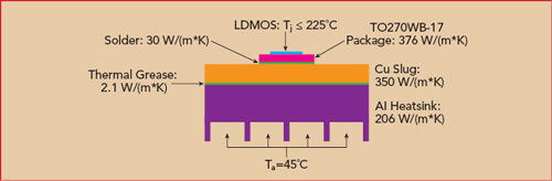
Figure 4 Assembly stack for thermal modeling.
Accommodating TDD
For fastest time-division duplex (TDD) switching, the gate capacitance should be minimized to below 1 nF, adding a series resistance (~50 Ω) on the gate bias feed to dampen any overshoot on the transitions (see Figure 5). On RF envelope peaks nearing transistor saturation, Schottky diode current on the gate can momentarily surge to 100 mA, so some charge storage is needed on the gate.
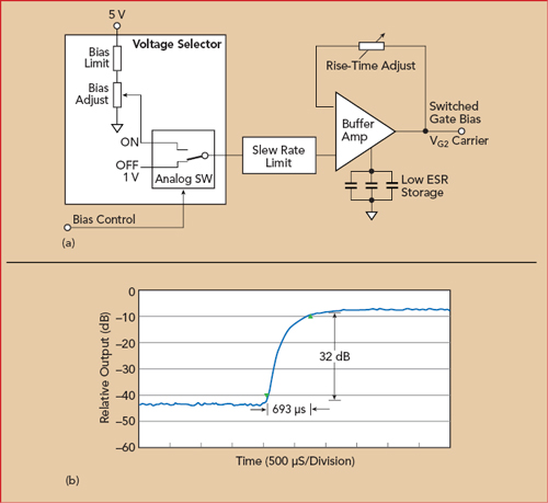
Figure 5 Gate switching circuit (a) and output power response (b) for TDD operation.
DESIGN VALIDATION: CBRS PA
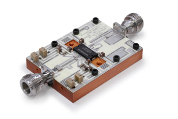
Figure 6 A3I35D025WN PA test fixture.
Using the dual-stage A3I35D025WB in a symmetrical Doherty configuration, a PA was designed for TDD operation in the CBRS band (see Figure 6). DPA performance with a CW input signal and without DPD is shown in Figure 7and summarized in Table 3. Figure 7a shows the gain compression at 3400, 3600 and 3800 MHz, and Figure 7b shows the drain efficiency vs. output power at the same three frequencies.
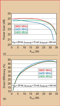
Figure 7 Output power vs. power gain (a) and drain efficiency (b) at 3400, 3600 and 3800 MHz.
Driven by two carriers, the linearity performance of the DPA at 3600 MHz, with and without DPD, is shown in Figure 8. At 3600 MHz, with two, 20 MHz LTE carriers separated by 200 MHz and 7 dB peak-to-average ratio, the DPA achieves 6.61 W average power with 37.1 percent efficiency and 24.5 dB power gain. The adjacent channel leakage power is −56.8 dBc at ±20 MHz offset from the carrier, −58.6 dBc at ±40 MHz offset and −59.3 dBc at ±60 MHz offset.
The ISBW of this DPA is greater than 300 MHz, which enables it to use DPD linearization over the full CBRS band. Depending on the DPD friendliness of the DPA, the DPD may require the output ISBW to be as much as 3 to 5x the baseband frequency to adequately sense the amplifier’s dominant intermodulation products. The ISBW requirement for DPD can be relaxed somewhat if the DPA has other favorable aspects of DPD compatibility. The DPD system may be sensitive to the symmetry of the IMD products, variation in gain compression characteristics (AM-to-AM and AM-to-PM) across the tuned band and memory effects.
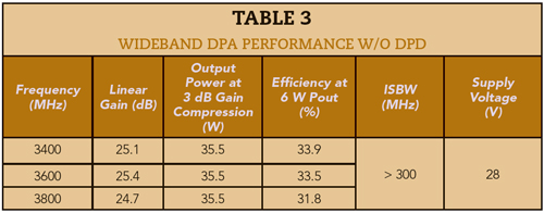
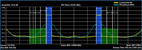
Figure 8 PA linearity with and without DPD.
SUMMARY
This article discussed the design of a symmetrical, wideband DPA for the CBRS band, reviewing the fundamental theory of DPAs and covering the design approach to optimize the performance of the carrier and peaking amplifiers and the overall DPA. The importance of ISBW for wideband operation with DPD was discussed, including design approaches to maximize the ISBW and the compatibility of the device technology to DPD. Using a commercial, two-stage LDMOS MMIC from NXP, the DPA delivered 6.61 W average output power with 37 percent efficiency, 24.5 dB gain, adjacent channel leakage of −56.8 dBc at ±20 MHz offset and greater than 300 MHz instantaneous signal bandwidth - suitable for covering the full 3550 to 3700 CBRS band.