
In the world of LTE, developers are very familiar with the available filtering technologies that work, namely surface acoustic wave (SAW) and bulk acoustic wave (BAW) filters. These filters cover a range of frequencies up to 6 GHz, come in small sizes and offer good performance-to-cost trade-offs, making them the dominant off-chip approaches in mobile devices today. Unfortunately, analogous filtering options for the mmWave spectrum have issues regarding viability, performance, size and availability, while research teams helping to write 5G standards have yet to provide information on what filters will be required, where they need to be placed in the base station and what performance metrics they must meet.
CONSIDERATIONS
The obstacles to and advantages for using the mmWave spectrum are both widely-publicized and well-understood. High frequencies suffer from range limitations and path loss through air, objects and buildings. However, mmWave signals require much smaller antennas, which can be tightly packed together to create single, narrowly focused beams for point-to-point communication with greater reach. Frequency bands around 28, 38 and 72 GHz are the main candidates for 5G mmWave, having demonstrated directional antenna, beamforming and beam tracking performance in multipath environments.1-2
The focus has now shifted to solving the practical issue of how to build an actual mmWave-capable base station and implement high performance RF filtering. Fortunately, mmWave technology has been employed for decades in various fields and functions. For example, it has a long history in military, aerospace and SATCOM applications such as K-Band inter-satellite communication and ranging and Ka-Band high-resolution radar.
In other industries, the automotive field is using both 24 GHz in short-range and 77 GHz in long-range radar-based advanced driver assistance systems (ADAS) to scan a vehicle’s environment for driver support or automated driving. In the U.S., 36 to 40 GHz is currently licensed for high speed microwave data links between a cellular base station and a base station controller; and, the unlicensed 60 GHz band is used in short range data connections and IEEE 802.11ad WiGig for high bandwidth streaming.
FILTER REQUIREMENTS
Chief concerns of industry leaders include:
- Quality and Performance: Can the filter perform accurately, repeatably and reliably across thousands of units?
- Time-to-Market: 5G deployment is nearly at hand, so do we have a solution that is available today for rapid prototyping and product development?
- Ease of Integration: Will the new filter solution be relatively straightforward to implement into existing technology? Can it be easily adapted for use with various wireless standards and frequencies?
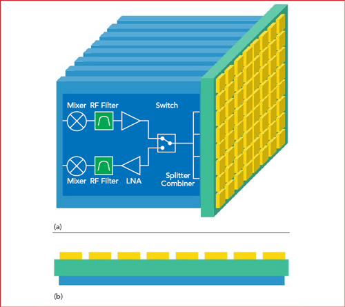
Figure 1 Alternative array architectures: plank (a) and flat panel (b).
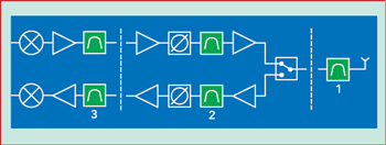
Figure 2 Potential radio filter locations.
Specific filter performance metrics must address the following:
- Percent Bandwidth: The filter technology must not limit the radio access system bandwidth.
- Selectivity: High selectivity enables designers to make good use of available bandwidth.
- Insertion Loss: Power is a system cost driver and on the receiver side, insertion loss impacts the overall noise figure of the receiver.
- Size and Packaging: In phased arrays, the antenna elements must be sufficiently close together to avoid generating grating lobes; a half wavelength spacing for mmWave frequencies amounts to only a few millimeters. As shown in Figure 1, phased arrays often used in mmWave applications use a plank architecture, in which the gold areas indicate the antennas mounted on a printed circuit board (PCB) (green area) and the blue areas indicate the circuit “planks” extending 90 degrees from array (where space for filters is already very limited). Base station manufacturers, however, are now looking into flat panel architectures where the circuitry is implemented on the back side of the antenna PCB, requiring even denser spacing for filtering and other functional blocks.
- Temperature Stability: In order to make efficient use of available bandwidth, the filter must meet its specifications over a range of temperatures. Small-scale systems may be deployed in exposed environments that experience extremes in temperature and temperature variation. Further, overall size reduction in systems leads to densely populated boards, where heat from surrounding components can affect filter stability.
- Power Handling: The ability of the filter to withstand large amounts of transmit RF power is mostly a concern in traditional macro-cell use cases below 3 GHz. In mmWave 5G use cases, the transmit power is spread over the individual array elements and the transmit range is reduced as well.
- Filter Placement: As shown in Figure 2, there are several practical locations: at the antenna element (Position 1), behind the amplifiers closest to the antenna (Position 2) and on the high frequency side of the mixers (Position 3). It should be noted that the dashed lines represent potential 1:N branching in a beam forming architecture, and that Figure 2 shows a simplified single path from mixer to antenna. The advantage of the Position 1 implementation is that linearity and bandwidth design constraints for the subsequent blocks is eased, potentially reducing overall system cost. Filtering placed at Position 1 suppresses noise far from the channel of interest across a wide frequency range, making wideband suppression and very low insertion loss key performance features. Given that each sub-array has its own filter, small size and low cost are important.
SOLUTIONS
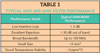
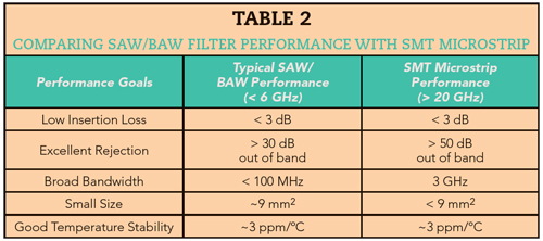
SAW and BAW filters have long dominated the off-chip filtering market in mobile devices because of their excellent performance specs, tiny footprints and affordable prices compared to other options. Unfortunately, the nature of their design - using interdigital transducers (IDT) to process signals as acoustic waves - exhibits degradation in selectivity at frequencies greater than 6 GHz, making SAW and BAW technology unfeasible for mmWave applications. Nevertheless, it is worth noting their performance metrics (see Table 1) as a benchmark for potential mmWave filter solutions.
Emerging SAW/BAW Alternatives
Given the successful use of SAW and BAW technologies at lower frequencies, researchers are naturally looking into developing an acoustic equivalent for mmWave applications.
The Film bulk acoustic resonator (FBAR) filter is a form of BAW filter that can reportedly operate from 5 to 20 GHz,3 which is applicable for LTE but still below desired mmWave ranges. Resonant Inc. is developing a so called XBAR™ technology that seeks to outperform FBARs, but currently it is only available as licensable intellectual property for manufacturers to complete development.
The use of substrate integrated waveguides (SIW) offers another approach where researchers seek to create small waveguide cavity filters for use in PCB and on-chip applications. While attractive for its wideband properties, good isolation and lower losses, challenges for mmWave include radiation leakage between plated through-holes (PTH), difficulties designing SIW transitions and dimensional variations in the PTH side walls (which are detectable at mmWave frequencies).4
Micro-Electro-Mechanical Systems (MEMS) offers the potential for tiny, tunable RF filters created using conventional semiconductor fabrication processes. The methodology is interesting due to its dimensional accuracy, high component density and low-cost at high volumes;5 however, current designs are still in the research phase or are limited to the sub-mmWave ranges.
Proven Approaches
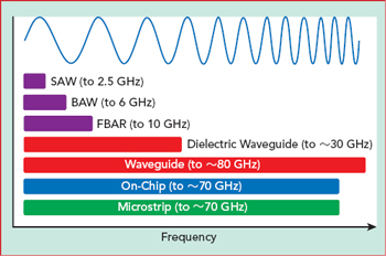
Figure 3 Frequency ranges of common filter technologies.
Figure 3 summarizes the frequency ranges of today’s commonly available filters. At higher mmWave frequencies, acoustic filtering is not as practical, so many developers have turned to electromagnetic (EM) solutions. For mmWave applications at 20 GHz and higher there are dielectric and cavity waveguide, on-chip and microstrip (or planar thin film) filters.
Waveguide filters are hollow or dielectric filled cavities within metal tubes that act as BPFs, blocking certain wavelengths while allowing others to pass. Characterized by high-power handling and low loss, waveguide filters are widely used for mmWave frequencies from 20 to 80 GHz in military, radar, satellite and broadcasting markets. Unfortunately, waveguides typically have dimensions in the centimeter range (see Figure 4). A λ/2 array element spacing at 28 GHz in free space is 5.35 mm. Until manufacturers are able to sufficiently reduce waveguide sizes while still meeting electrical performance requirements, this solution may not be practical for an array antenna system.
On-chip filters using semiconductor technologies are attractive because of the compact circuits, tight tolerances, and the capability for integration with other devices to form system on a chip (SoC) solutions. Yet, significant performance issues regarding Q-factor, losses and noise figure (NF) occur with the production of on-chip devices having reduced dimensions for mmWave frequencies.

Figure 4 Sizes of mmWave filters compared to typical SAW filters.
Challenges arise from various factors, including the physical characteristics of the semiconductor material and the cost of implementation. For example, GaN circuits are made as thin as possible to increase heat dissipation; however, filter Q is proportional to dielectric substrate thickness, so the high-power advantage of using GaN devices works in opposition to integrating filters with high Q. In addition, a filter structure in GaN occupies valuable real estate on the wafer that would be better allocated to active devices. Building on-chip high Q filter structures to serve in a front-end application is currently impractical.
Microstrip filters have been considered for mmWave applications but are commonly dismissed for various performance issues. Note that there are at least three different form factors:
- Microstrip on PCB
- Microstrip in a multilayer, low temperature co-fired ceramic (LTCC) package
- Microstrip in a small form factor, single-layer package
Microstrip filters printed on PCB are appealing because of their simple construction, but high performance PCB solutions generally reach centimeter-range sizes, which are much larger than the sub-wavelength dimensions required for mmWave antennas. Variations caused by the PCB manufacturing processes also limit performance, resulting in higher insertion loss and lower suppression values.
Another option is surface mount technology (SMT). SMT assembly has been long used in commercial systems and is now being adopted in mmWave military systems for potential cost savings. Unlike chip and wire solutions, SMT filters have standardized form factors to reduce overall assembly time, and require no post-tuning. Figure 5 shows the performance repeatability of 100 SMT BPFs, measured in the 26.5 to 29.5 GHz range without tuning.
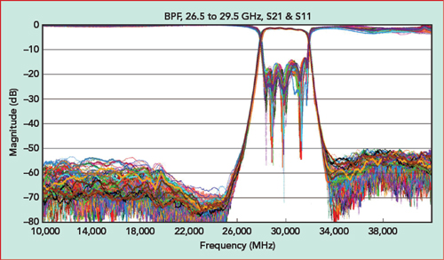
Figure 5 Repeatability of Knowles Precision Devices 28 GHz SMT single-layer microstrip filters, using 100 samples without tuning.
LTCC filters come in a SMT form factor and are similar to multilayer capacitors, in which multiple layers of very thin ceramic tape are printed with different passive elements and then stacked together to prevent substrate warping. Prototypes of LTCC technology for mmWave applications are being developed, potentially offering a method of including both filters and antennas on the same component with a very small footprint. Unfortunately, since the metal coatings are screen printed, dimensional precision is not as high as other thin film solutions and the unpolished substrate can lead to high losses.6 Plus, suppression is generally limited to 30 dB and below.
Another type of SMT filter assembly is single-layer microstrip, which is printed with distributed transmission lines to create high performance resonant structures. With a careful choice of filter topology and dielectric materials, high rejection, low loss filters that are temperature stable from −55°C to 125°C can be produced. These filters provide performance similar to their lower frequency SAW and BAW counterparts (see Table 2). High performance and small form factor devices are possible within the constraints of 5G New Radio (NR) systems. Figure 6 shows the functionality of a low loss 26 GHz filter with greater than 50 dB of suppression that fits in a 4 mm x 1.6 mm footprint. This size is significantly smaller than half a wavelength, enabling integration in both plank and planar architectures.
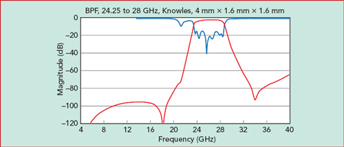
Figure 6 Performance of a Knowles Precision Devices 26 GHz single-layer 6.4 mm2 microstrip BPF.
CONCLUSION
The timeline for delivering mainstream 5G communications is getting tighter, and determining the appropriate RF filtering for 20 GHz and above is a fundamental issue. 5G systems require filters with high percentage bandwidths, good selectivity and excellent temperature stability in compact packages. In order to accelerate time-to-market, developers are seeking established solutions, such as waveguide and microstrip filters, that have long been used in the satellite, radar and broadcasting industries.
References
- T. S. Rappaport, “Millimeter Wave Cellular A Road to 5G,” IEEE International Conference on Communications,” June 2013, https://wireless.engineering.nyu.edu/presentations/icc2013.pdf.
- K. Sakaguchi, T. Haustein, S. Barbarossa, E. C. Strinati, A. Clemente, G. Destino, A. Pärssinen, I. Kim, H. Chung, J. Kim, W. Keusgen, R. J. Weiler, K. Takinami, E. Ceci, A. Sadri, L. Xain, A. Maltsev, G. K. Tran, H. Ogawa, K. Mahler and R. W. Heath Jr., “Where, When, and How mmWave is Used in 5G and Beyond,” IEICE Transactions on Electronics, Vol. E100-C, No. 10, October 2017.
- “5G NR Primer for Amplifier and Filter Design,” National Instruments, September 2018, www.awrcorp.com/news/article/5g-new-radio-primer-amplifier-and-filter-design-now-available.
- J. Conrood, “Substrate Integrated Waveguides (SIW) Limits and Capabilities,” Rogers Corp., January 2018, www.youtube.com/watch?v=I9A66sUqaTk.
- T. Pensala, “MEMS & Thin Films Manufacturing Platform for Mm-wave and 5G RF Components,” Eemeli Workshop, May 2015, www.vttresearch.com/Documents/Eemeli/20th%20Eemeli/05%20Pensala%20Eemeli%2021.5.2015%20mm-wave%20MEMS%20thin%20film%20manufacturing%20platform%20VTT%20TPensala.pdf.
- N. Friedrich, “The Do’s And Don’ts Of LTCC,” Microwaves & RF, September 2013, www.mwrf.com/passive-components/do-s-and-don-ts-ltcc.