
Small size and component integration are key goals for high frequency phased array radars. As system frequencies increase, array element spacing reduces and the area for the RF front-end driving each element also shrinks. Addressing these needs, Qorvo’s QPM1002 is a single-chip X-Band front-end module (FEM) for radar applications from 8.5 to 10.5 GHz. The MMIC integrates a T/R switch, low noise amplifier (LNA) and power amplifier (PA) on a single GaN MMIC (see Figure 1).
The QPM1002 is fabricated on Qorvo’s 0.25 μm GaN on SiC process and encapsulated in a 5 mm × 5 mm plastic overmolded QFN, which minimizes cost, maximizes moisture robustness and simplifies next-level assembly. The compact size supports the tight lattice spacing of X-Band phased array radars and is also advantageous for electronic warfare and communication systems.
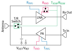
Figure 1 The QPM1002 front-end integrates an LNA, PA and T/R switch and connects to the antenna.
In receive (Rx), the FEM provides 25 dB gain with a low noise figure of 2.2 dB (see Figure 2), with the typical input and output return loss around 13 and 12 dB, respectively. In transmit (Tx), the FEM has 33 dB small-signal gain and delivers 3 W saturated output power, 32 percent power-added efficiency and 25 dB large-signal gain (see Figure 3), with the typical input and output return loss 15 dB. The Rx and Tx performance include the losses and mismatch associated with the T/R switch. The MMIC includes an on-chip output power detector with a 0 to 0.3 V output proportional to transmit power. The FEM is robust and will handle up to 2 W power applied to the antenna port, eliminating the need for a limiter to protect the LNA in most systems. A photograph of the QPM1002 mounted on an evaluation board is shown in Figure 4.
The QPM1002 is classified as EAR99 for export, meaning it can be exported to qualified international customers.
GaN ADVANTAGES
An all-GaN MMIC solution offers several advantages:
- GaN is robust, with an operating temperature range of ‐55°C to +100°C.
- GaN LNAs can survive high incident RF power, eliminating the need for an Rx limiter in front of the LNA.
- The all-GaN solution minimizes size and simplifies system integration.
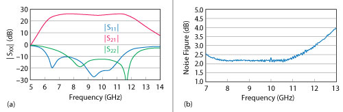
Figure 2 Gain, |S11|, |S22| (a) and noise figure (b) of the LNA path at 25°C.
Rx robustness was tested at 95°C by driving successively higher input power into the antenna port for three minutes at each power level. Based on test results, the QPM1002 has a maximum antenna port input power rating of 2 W. PA robustness was similarly tested by driving it into saturation with highly reflective loads at the antenna port. The PA withstands a 10:1 load while driven into saturation without failure or degradation.
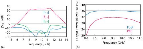
Figure 3 Gain, |S11|, |S22| (a) and output power and PAE (b) of the Tx path at 25°C.
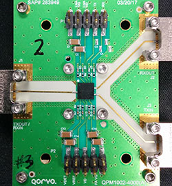
Figure 4 The QPM1002 surface-mounted to the evaluation board. A copper-filled via array underneath the module improves heat conduction from the device.
When the QPM1002 is in the Tx mode, on-chip circuitry turns off the current to the drain of the LNA using the Tx/Rx control lines (shown in Figure 1). This reduces the chance of LNA damage during Tx operation and increases the isolation of signals leaking through the LNA to the Rx output. The LNA turn-off circuitry conveniently eliminates the need for gate/drain switching on the LNA when changing from Tx to Rx or vice-versa.
The typical output power of a GaN LNA is greater than 25 dBm, which could require attenuation or other power-limiting circuitry if downstream components are sensitive to power levels of this magnitude. To avoid this issue, the QPM1002 LNA implements a novel topology to limit the output power to 17 dBm, even when heavily saturated and at cold temperatures. This allows the LNA to directly drive sensitive SiGe beamformer ICs, which typically have maximum input power ratings of 17 to 18 dBm.
OPTIMIZED ANTENNA PORT SWITCH
The T/R switch topology was optimized to minimize the Rx noise figure and maximize Tx power-added efficiency; both are heavily influenced by the respective networks interfacing with the SPDT switch. The best performance was achieved by absorbing the off-state switch capacitance into the PA output and LNA input matching networks.
Qorvo
Greensboro, N.C.
www.qorvo.com