

CST STUDIO SUITE Complete Multi-Domain and Multiphysics Solution
Dassault Systèmes, SIMULIA CST, Darmstadt, Germany
SIMULIA’s CST STUDIO SUITE is a 3D design environment that enables access to EM and multiphysics simulation. Fully parametric models can be constructed in CST STUDIO SUITE or imported through the interface with leading CAD and EDA design tools. Entire EM systems can be designed from their constituent components using the CST System Assembly and Modeling (SAM) framework. Parameter sweeps allow different design configurations to be analyzed in a single simulation flow, while the built-in automatic optimizers can be used to tune and improve the performance of devices.
With Filter Designer 3D, CST STUDIO SUITE features a dedicated design flow, allowing even extremely complex filters to be tuned, with multiple passbands and transmission zeroes, if required. CST’s fast resonant solver and innovative moving mesh method offer smooth convergence, allowing even very sensitive filters to be optimized efficiently. These approaches can save both time and money compared to traditional physical testing, by reducing the number of prototypes required to achieve a design that meets the requirements.
Multiphysics simulation can be important for high-power devices, where excess heat due to EM losses in materials can cause damage and expansion and deformation that detune sensitive components such as filters and resonators. To allow these effects to be simulated and mitigated from the earliest stages of the design process, CST STUDIO SUITE offers integrated thermal and structural mechanical solvers capable of simulating temperature distribution, heat flow, cooling, biological heat effects and thermal expansion.
Once the individual components have been designed, the work of the system integrator begins. For a complex product such as a car, multiple components can be imported from different tools—the car body from one source, the cable harness network from another, the circuit boards from yet another and the communication and radar antennas from the CST antenna tool Antenna Magus—and assembled into a simulation project using SAM.
Antennas and other parts need to be placed in the system in such a way that they work as intended, in what is often a challenging and crowded environment. The metal body of a car or aircraft will affect the radiation pattern of antennas placed on its surface, while the human body can absorb or reflect energy from handheld and wearable devices. CST STUDIO SUITE includes several methods suited to simulating antennas on electrically large platforms, which can be used to calculate the performance of individual antennas and the coupling between multiple antennas (see Figure 7).
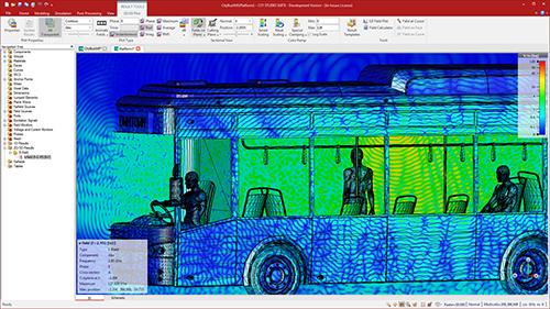
Figure 7 Simulated electric fields of an antenna placed on a bus in the CST STUDIO SUITE interface.
EMC and EM interference (EMI) are significant concerns in product design. If not caught as early as possible, installed performance and interference problems can significantly delay the development of a product or require costly and reputational damaging recalls. With the new CST Interference Task, potential interference problems can be identified at the design stage, helping ensure compliance with legal regulations and reducing the risk of unexpected issues emerging during testing.
For devices used near the body, there are also legally-mandated limits on the exposure to RF fields, measured as specific absorption rate (SAR). These, too, can be simulated with CST STUDIO SUITE to check design compliance with regulations.
By integrating all these features into one user interface, CST STUDIO SUITE helps engineers optimize their designs quickly and efficiently and avoid problems that can add to the development time and cost of a project. With CST STUDIO SUITE 2018, CST, now part of the SIMULIA brand of Dassault Systèmes, is integrating its software with the 3DEXPERIENCE platform, which connects CAD, PLM, collaboration and other leading edge simulation software, to provide a complete multi-domain and multiphysics solution.
Keysight PathWave Design--More Creativity, Less Busywork
Keysight Technologies, Santa Rosa, Calif.
Board designs are becoming increasingly complex, with increased substrate layer counts, smaller form factors and limited design space. Additionally, once a design is complete, the designers still need to handle all the logistics, handoffs and liability, making it difficult to spend enough time actually designing and creating new products. To avoid frustration and spend more time innovating, engineers need a way to streamline their workflows.
Keysight’s design platform enables designers to focus on their favorite part of the job: the creative design process. Keysight PathWave Design is a new design environment that gives engineers the space for creativity, data displays for validation and common data formats to share ideas with colleagues. It provides integrated system, circuit and EM simulators, plus optimizers and layout capabilities that seamlessly integrate to save time and frustration in investigating various aspects of the design (see Figure 8).
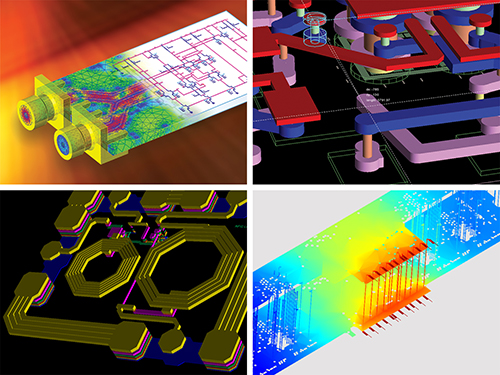
Figure 8 Keysight PathWave Design offers a variety of libraries, simulators, optimizers, layout views and data displays so design engineers can focus on creating and designing.
Keysight PathWave Design is built on Keysight Advanced Design System (ADS) and other software offered by Keysight EEsof EDA, including EMPro for EM analysis, SIPro for signal integrity analysis and PIPro for power integrity analysis. A benefit of designing with Keysight is the measurement expertise, depth of understanding the standard specifications and breadth of component libraries. The industry-compliant wireless libraries enable verifications of designs to all the latest wireless standards: 5G, LTE-A, 802.11ac, PCI Express, USB 3—and whatever standards the future brings will be added.
A design engineer’s work is not done once the design is complete. The handoff to the design verification test team is not just a simple handshake. Years ago, designs were less complex and specifications less stringent and a simple linear product development lifecycle pipeline worked. But today, the product development lifecycle has been transformed into a matrix of complex relationships between the design, verification and test teams. This is where the power of the Keysight PathWave Platform shines: it not only contains a design environment, but a test environment with common data formats, a consistent user experience and similar control interfaces. It is this integration that bridges the design and test engineers’ worlds, allowing them to speak the same language and interact in a completely new way (see Figure 9).
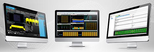
Figure 9 PathWave Design and PathWave Test eliminate silos between design, verification and test teams, allowing engineers to share data between multiple software programs as shown here for 5G NR signals.
PathWave Test is a test automation environment that optimizes test plans and operates with third-party hardware to provide seamless data transfer and analytics to the design environment and to the manufacturing teams. This makes it much easier for the test teams to go back to the design engineers and let them know of possible problems. This reduces time spent and eases communication in design iterations and troubleshooting, for both design and test engineers.
Both the PathWave Design environment and PathWave Test environment live inside the PathWave Platform, a systems engineering platform that eliminates silos between design, test and manufacturing teams, providing data and immediate insights to accelerate the product development lifecycle. In the future, PathWave will be what a student thinks of when visualizing a design becoming reality.