
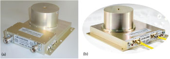
Figure 1 2.856 GHz PL-DRO (a) and 3.9 GHz DRO (b).
Two designs of ultra-low noise dielectric-resonator oscillators (DRO) for 2.856 GHz1 and 3.9 GHz2 with sub-femtosecond jitter (shown in Figure 1) are reviewed. This work was motivated by contracts with research institutions Deutsches Elektronen-Synchrotron,3 Hamburg, Germany and Pohang Accelerator Laboratories,4 Pohang, Korea that require this level of performance for optimum operation of their X-ray Free Electron Laser (X-FEL) installations. However, other applications like the microwave synthesizers found in Caesium-Fountain atomic clocks or high performance radars also may benefit from ultra-low noise signal sources of this kind. And the design methodology presented can, in principle, be transferred to any frequency in the 1 to 20 GHz range.
X-FELs are still a rare breed of research facilities, with just four installations worldwide that are capable of generating extremely intense (GWatts), ultra-short (20 to 50 fs) flashes of coherent radiation, reaching down to and below 0.1 nm wavelength (see Figure 2). These short-wavelength (“hard”) X-rays are in high demand by researchers for imagery at the molecular, atomic and even subatomic level.5-6 Even more unique, the ultra-short flashes allow sampling of the dynamics of atomic bonds or chemical reactions to generate video-like sequences of those picosecond processes7-8 at the atomic level.
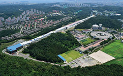
Figure 2 Aerial view of the PAL X-FEL at Pohang, Korea (courtesy PAL4).

Figure 3 Simplified X-FEL block diagram.
X-FELs work by accelerating bunches of electrons to extremely high energies (10 to 20 GeV) and converting a small amount to coherent X-rays of a very narrow spectral range. The “lasing” action takes place in a long chain (> 100 m) of alternating polarity magnets, called “undulators,”9 and requires the accelerated electrons to have a very small energy spread (see Figure 3).
The acceleration process makes use of a microwave signal (mostly 2.856 or 1.3/3.9 GHz), distributed throughout the installation and amplified in many substations to tens of megawatts of pulse power. Each high-power amplifier drives a group of cavity resonators, (forming a long chain of up to 1700 m), with their extremely large electromagnetic fields propelling the electrons forward. For optimum energy transfer, the phase relationship of the microwave signal must be precisely matched to the locus of the electron bunch. Phase stability to 0.01° (10 fs at 3 GHz) is needed for optimum acceleration with minimal energy spread and the ability to compress the electron bunch down to femtosecond duration and maintain it.
The targeted phase stability requires extremely stable signal sources, containing jitter ideally to just a few femtoseconds. But how does this relate to phase noise, the quantity usually used to describe the short term stability of a signal source?
Jitter versus Phase Noise
While the phase noise spectral density function L(fm) completely describes the short term stability of a signal source, phase jitter, the measure of the output waveform zero-crossing’s time deviation, is computed by integrating L(fm) over a certain offset frequency range, implying that jitter numbers must always be accompanied by that integration range and can only be compared when the integration ranges match.
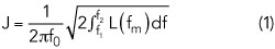
Computing jitter with Equation 1 neglects all contributions of the phase noise spectrum below f1 and above f2 and is well justified, if f1 and f2 are chosen in a meaningful way for a given system. Typically a system has a “maximum observation time,” defining f1 (slower phase changes do not alter the system’s output) and a “maximum processing bandwidth,” that sets f2 (faster phase changes are not processed by the system).
In FELs, the processing bandwidth ranges from10 to 30 MHz, with 100 MHz on the horizon, giving a first hint at what to look for in designing a low jitter signal source, as the higher f2, the more important a low oscillator noise floor becomes.
With the lower bound f1 typically specified as 1 Hz, to ensure pulse to pulse stability and keep low frequency noise from interfering with drift countering measures, signal sources for FELs are always a combination of a microwave oscillator that defines phase noise from 1 to 10 kHz to f2, phase locked to quartz crystal oscillators, determining phase noise from 1 Hz to 1 to 10 kHz. For the oscillators discussed here, jitter numbers integrating phase noise over 1 kHz to 30 MHz or 10 kHz to 30 MHz are relevant.
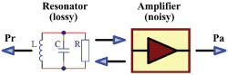
Figure 4 Reflection oscillator topology.
Ultra-Low Phase Noise Oscillator Design
There are only a few elements needed to build an oscillator: a (lossy) resonator to set the frequency, an amplifier to compensate the resonator’s losses and both arranged in a feed back loop.
Oscillator Topologies
The first decision in designing an oscillator involves how the amplifier and resonator are coupled in a feedback arrangement. Most oscillators use the “reflection” type topology shown in Figure 4 (negative resistance oscillator10). Note the possibility of either taking the oscillator’s output power (Po) from the amplifier (Pa) or coupling to the resonator (Pr). This topology, albeit simple, has the drawback that a number of important parameters like resonator loading, output power and amplifier compression are tightly coupled and hard to control separately.
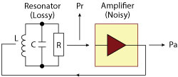
Figure 5 Transmission oscillator topology.
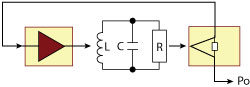
Figure 6 Optimum transmission oscillator topology.
For narrowband sources, the topology of a transmission type oscillator, shown in Figure 5, gives much better control of the critical parameters, is widely used11-13 and chosen here. Again, the designer has the choice to take the output power from the amplifier (Pa), maximizing Po, or from the resonator (Pr). The latter reuses this element as a filter to suppress the amplifier’s broadband noise outside the resonator’s passband,12,14 outweighing the loss of signal power that is easily compensated by a following buffer amplifier. Using this topology (see Figure 6) is key to achieving low noise floors of -180 dBc/Hz (see trace 6 in Figure 7).
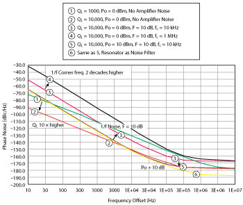
Figure 7 Oscillator phase noise from Equation 2 with varying parameters.
Oscillator Optimization for Low Noise
For determining what measures need to be taken to arrive at a low noise, low jitter oscillator, the old phase noise model of Leeson15 is still helpful:

It relates the single sideband (SSB) phase noise L (in dBc/Hz) as a function of the offset frequency fm around centre frequency f0 to four important parameters. To minimize noise, this model dictates:
- Maximize S/N in the loop, by maximizing signal power PS with respect to noise power FkT (F: noise factor).
- Maximize the loaded Q QL=f0/BW3dB of the resonator.
- Minimize the amplifier’s flicker corner frequency fc.
Figure 7 shows a number of simulated phase noise diagrams and the influence of those four parameters. Obviously, optimizing QL is of most efficiency, as it enters Equation 2 squared. Less obvious, the highly device technology dependent fc can have a huge impact, as it is not unusual to find GaAs devices to have 100x higher 1/f-noise corner frequencies than their silicon counterparts.