
From metallic alloys to plastic composites, scientists and engineers have been developing artificial materials for various applications. Metamaterial, a family of artificial composite structures made from conventional material with unconventional structures, exhibits distinct properties apart from what nature can provide easily, such as negative index characteristics for selective frequency regions.1-8 The shape, size, geometry, orientation and arrangement of metamaterial gives it smart properties, capable of manipulating electromagnetic (EM) waves by bending, blocking, absorbing and enhancing to attain benefits that go beyond what is possible with conventional materials.
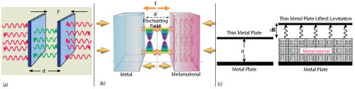
Figure 1 The Casimir force (F) on a parallel plate kept in vacuum (a)9 the repulsive Casimir force (F) on parallel plate (b)11 Casimir force levitating a mirror (c).12
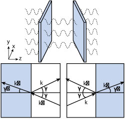
Figure 2 The Gravitational Casimir effect.13
Metamaterial structures that show Möbius symmetry, where coupling strengths and size of the structure scales can be engineered, are promising candidates for next generation electronics in lower profile and energy saving electronics.2 Distinctive contributions in the field of Möbius Metamaterial Inspired (MMI) technology allow topological exploration, yielding high Q factor, based on evanescent mode resonance.3 The reported multi-knot Möbius Metamaterial Strip (MMS) structure enables multi-injection-nodes for multi-phase-injection-locking, facilitating concurrent signal-source solutions.4 MMI based technology enables energy harvesting for the realization of next generation energy-saving for spintronic devices, quantum oscillators, RFID, signal retention devices and proximity sensors; as well as providing enhanced dynamic range for underground detection, detection of trapped victim heartbeats and biosensor applications.5-6
What makes an MMI structure unique is its topology and size. It interacts with forces at the nanoscale, so that interface dynamics can be explained by quantum mechanics. The same structure scaled much larger than its wavelength would no longer exhibit the same properties. Its characteristics can be described by conventional structural engineering and material science. At the nanoscale, an MMI structure can exhibit the repulsive Casimir force,9-11 which has important practical applications in creating anti-gravity and levitation.12 Figure 1a shows the Casimir force ‘F’ on parallel plates in a vacuum, the effective force F is proportional to A/d4, where A is the area of plate and d is the distance between the plates.9 It can be either an attraction or a repulsion depending on the specific arrangement of the two plates. Figure 1b shows the repulsive Casimir force ‘F’ on parallel plate kept in vacuum,11 while Figure 1c shows how this can be used to balance the weight of a mirror.12

Figure 3 The Internet of Things.14
The Casimir force arises from the interaction of the surfaces with the surrounding electromagnetic spectrum, and includes a complex dependence on the full dielectric function of both surfaces and the region between. The complexity of the Casimir force leads to significant possibilities for manipulation through materials, geometries and other phenomena. It potentially provides the opportunity for neutralizing or partially cancelling Van Der Waals forces. On the more theoretical side, the MMI structure can produce a powerful Casimir effect (force from nothing), which enables the transport of matter, i.e., the use of this effect to attract or repel physical matter. Some practical applications include auto focusing camera lenses, more efficient servos, silicon array propulsion systems and high speed rail systems. The implications of a repulsive Casimir force for the micro-electromechanical systems (MEMS) industry could be significant with potential applications including stiction prevention in sensors, contactless bearings and contactless power transmission.10 MEMS based electronics offer inexpensive high performance solutions; but reliability issues arising from stiction in MEMS switching devices limits their use in high frequency applications.
The pioneering contributions relate to techniques for a stiction-free MEMS lateral switch and its application in switching networks and phase shifters in electronically scanned phase array antennas for Internet of Things (IoT) applications. In a vacuum, the force of attraction between two surfaces separated by nanometers is explained by the Casimir effect, but effective repulsive forces can be noticed when the two surfaces with materials of different permittivity are taken into consideration.11-12 This phenomenon can also be observed if one of the surfaces possesses negative permittivity. This approach can resolve the stiction problem, leading to new material and fabrication methods in next generation MEMS.
One of the exciting properties of MMI structures is that they can bend light in a way that is mathematically equivalent to the way space-time bends light, allowing topological exploration for the realization of low cost gravitational wave detectors. Figure 2 shows the Gravitational Casimir effect, with a two plate setup. The change in the refractive index of the plates causes the gravitational wave to refract, where k represents the wave vector of the incident, transmitted, and reflected gravitational waves, and γ is the corresponding angle with respect to the surface normal.13
Details of the Casimir effect and applications and use of the MMI structure for futuristic applications will be discussed in part 2 (June 2016 issue) and part 3 (July 2016 issue). This article briefly describes applications of the MMI structure for the IoT, CubeSat, and examples of the Möbius transformation and metamaterial symmetry for medical telemetry, imaging and sensor applications.
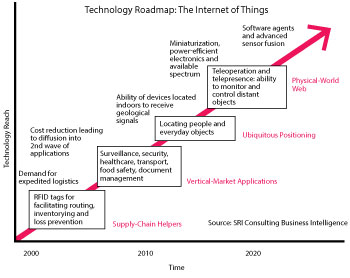
Figure 4 IoT Technology Roadmap.14
INTERNET OF THINGS (IoT)
The Internet of Things (IoT) is the network of physical objects: devices, vehicles, buildings and other items embedded with electronics, software, sensors and network connectivity that enable these objects to collect and exchange data (see Figure 3).14 The IoT allows objects to be sensed and controlled remotely across the existing network infrastructure, creating opportunities for more direct integration of the physical world into computer-based systems, resulting in improved efficiency, accuracy and economic benefit; when the Internet is augmented with sensors and actuators, it becomes an instance of the more general class of cyber-physical systems, which encompasses technologies such as smart grids, smart homes, intelligent transportation and smart cities. Each thing is uniquely identifiable through its embedded computing system but is also able to interoperate within the existing Internet infrastructure.
Figure 4 illustrates the IoT Technology Roadmap.14 Current technology cannot yet meet the needs for faster, more reliable and more ubiquitous radio systems required by the IoT. The trend over past decades has been to place an ever increasing emphasis on digital signal processing (DSP), where spectral efficiency has been maximized via sophisticated modulation, multiplexing or MIMO schemes. However, these approaches have now reached their limits and migration to millimeter wave and terahertz frequencies has become indispensable to access broader spectral resources. Unfortunately, DSP is not applicable at such frequencies, where signals are varying too fast to be digitized. The unprecedented control of electromagnetic properties afforded by the MMI structure opens the door to provide fast processing and low power miniaturized electronics to overcome technological challenges.
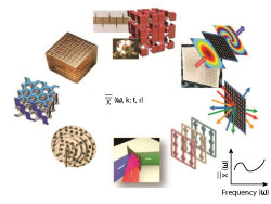
Figure 5 Sketch of metamaterial engineering.8
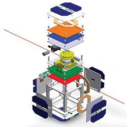
Figure 6 Typical CubeSat layout (courtesy ESTCube-1).18
Recent publications describe the real-time analog signal processing (R-ASP) of electromagnetic waves at very high frequencies using metamaterial inspired technology in conjunction with concepts of ultrafast optics.15-17 There is need for a special branch of metamaterial engineering concerning the manipulation of EM waves in space, time and space-time for the realization of an unlimited number of distinct types of artificial smart materials (electromagnetic band gap metamaterial, single negative metamaterial, double negative metamaterial, biisotropic and bianisotropic metamaterial and chiral metamaterial). This technology is suited for telecommunications, medical instrumentation (bio-medical, oral and oncology, ultrasound imaging and magnetic resonance imaging), optics, sensing (bio, thin film, wireless strain, aerospace and defense), energy harvesting, transportation of matter, and levitation/anti-gravity (attractive and repulsive Casimir effect).
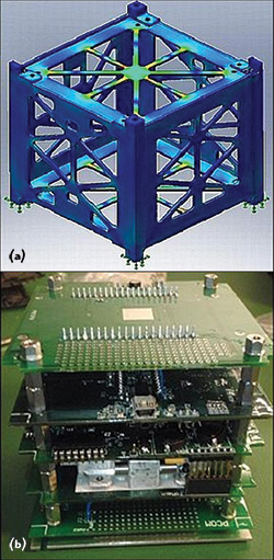
Figure 7 CubeSat bus structure (a) and photo of the interior bus configuration (b) (courtesy Colorado Space Grant Consortium).19
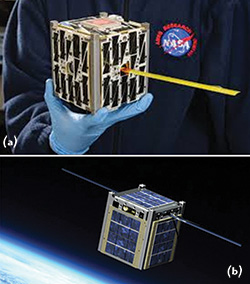
Figure 8 CubeSat hardware (a) and CubeSat in low-Earth orbit (b) (courtesy NASA).20
These applications are supported on the IoT technology roadmap.14 Figure 5 depicts the typical sketch of metamaterial engineering, illustrating the solutions for next generation electronic circuits and systems.8 As shown in Figure 5,  is the generic notation of tensors that represents the metamaterial permittivity (
 ), permeability (
 ), magnetic-to-electric coupling (
 ) and electric-to-magnetic coupling (
 ) tensors, while ωis the angular frequency (reciprocal time), k is the spatial frequency (reciprocal space), t is time (direct time) and r is space (direct space). Combining different dependencies (ω, k; t, r) and bianisotropies
  leads to a virtually unlimited number of distinct types of metamaterials.8

Figure 9 Network of CubeSats (courtesy NASA).20
CUBESAT
Satellites play a decisive role for establishing communication networks; these satellites are expensive, large in size and take a number of years to build up. To keep costs low, small satellites such as the CubeSat, have yielded big rewards versus their larger counterparts. Small satellites are located in low-Earth orbit (LEO) in the range of 200 to 2,000 km altitude. The speed of small satellites in LEO (relative to Earth’s surface) is around 7.5 km/s, which is an orbital period of approximately 90 minutes. The definition of CubeSat comes from its shape and weight. It belongs to the family of small satellites: Picosatellite <1 kg, nanosatellite 1 to 10 kg, and microsatellite 10 to 100 kg). Figure 6 shows a typical CAD model of a CubeSat (10 cm × 10 cm × 10 cm),18 Figure 7 shows a typical bus structure and Figure 8 shows the actual CubeSat in hand as well as its position in low-Earth orbit. 20 The basic subsystems of a CubeSat are telemetry, tracking and control (TTC), power generation and distribution (PGD), data command and handling (DCH), altitude determination and control (ADC) and the payload.
Small satellites cost much less per unit; many CubeSats can be fabricated for the price of one conventional satellite. Although a CubeSat is lower in cost, it obviously does not have the individual payload capacity of a large satellite. A possible cost-effective alternative is to launch many CubeSats as depicted in Figure 9, and construct a network of small satellites that can accomplish the same tasks as one large satellite. The advantage is that if one CubeSat fails, the network can be reconfigured to pick up the slack, whereas one satellite is a single point of mission failure. Figure 10 illustrates the CubeSat launch operations concept,19-22 while Figure 11 shows the communication link.23
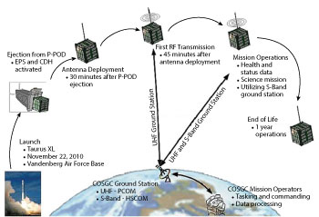
Figure 10 CubeSat launch operations concept (courtesy Colorado Space Grant Consortium).21
Antenna size for the communication link is a limitation in small satellites. The maximum gain of conventional aperture antennas (e.g., dish reflectors, horns, arrays) is determined by aperture size. The relatively large size needed for adequate performance, however, makes them unfriendly for space application. Modifications enabled by smart material can either enhance performance or reduce mass, thus lowering the cost of putting the antenna in space. Lighter antennas reduce weight directly, while more energy efficient antennas reduce the size and weight of required storage batteries and solar cells. The metamaterial lined horn antenna with low-index electromagnetic properties shown in Figure 12, for example, is relatively small in size, but not yet suitable for small satellite (CubeSat) applications.24
Ongoing research towards developing miniaturized low-index metamaterial lens antennas for small satellites faces challenges such as bandwidth and efficiency. Metamaterial lenses exhibit material properties that approximate the behavior of a material with low (0<n<1) effective index of refraction, and by using dispersion techniques a relatively wideband low-index region can be obtained. A low-index metamaterial lens can create highly collimated beams in the far field from a low directivity antenna feed by, for example, using dual-split ring resonators (DSRR) in the x-y plane for a low permeability response, and end-loaded dipole (ELD) elements in the x-z and y-z planes for a low permittivity response.
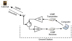
Figure 11 Schematic of general CubeSat communication setup.23
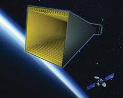
Figure 12 ypical metamaterial lined feed horn antenna for satellite communications.24
As ε or µ approaches zero, the passband narrows, improving collimation and directivity of the antenna, so that it can be integrated with software defined radio (SDR), facilitating a transformative communication system with remarkable frequency and polarization agility; this is well suited for CubeSat application where multifunctional miniature antennas is the desired goal.
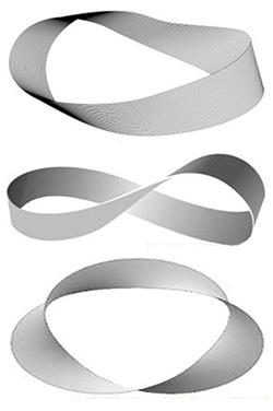
Figure 13 Möbius strips with single twist (top) with single twist and pinched (center) and with three twists (bottom).
Figure 14 Möbius strip symmetry in metamolecular trimmers.27
Smart MMI structures support the development of miniaturized multifunctional antennas, high efficiency solar panels for power generation and the performance of real-time analog signal processing of electromagnetic waves at very high frequencies. Tunable metamaterials using Möbius topology enable broadband tuning in a compact size with narrow instantaneous bandwidths across an entire communications band depending on the channel in use. Tuning the metamaterial and the antenna in tandem provides a dynamic operating channel with a tunable, nearly arbitrary polarization response as an added benefit. The major challenge is figuring out a way to scale these metamaterial and associated antenna structures to operate at lower frequencies while maintaining a practical physical size and weight. MMI technology enables a planar antenna with reduced size at lower frequency without degrading performance.
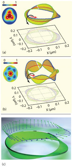
Figure 15 Numerically calculated and experimentally observed optical polarization twist around the Möbius strip: single knot (a)multi-knot (b) and polarization twist (c).28
MÖBIUS TRANSFORMATION: METAMATERIAL SYMMETRY
The concept of the Möbius strip is based on the fact that one can travel without encountering obstruction around the loop. The loop behaves like a never ending point, giving rise to the concept of an infinite path in the space-time domain. The concept of infinity is not emptiness or space; rather, it is the concept of having no beginning and no end (see Figure 13). As shown, the Möbius strip with one twist and pinched in the middle appears like the mathematical symbol for infinity. Since space-time is curved, it could conceivably run back on itself like the Möbius strip, and have no boundary. Our universe can be considered to be a replica of the Möbius strip with a multiple number of twists of vibrating strings in space, whirling in a warped loop as it experiences its own starting point, and recurs perpetually in space-time dynamics. These “strings” vibrate in multiple dimensions, and depending upon how they vibrate, they might be seen in 3-dimensional space as matter, light or gravity. The figure also shows a 3-twist Möbius strip (twists can be defined as knots).
For engineers, the multi-knot Möbius strip surface is a launch pad to complex geometries and topological exploration of next generation electronic circuits and systems for industrial, medical and space applications. Topology is a field of science that studies invariance of certain properties under continuous deformation, such as stretching, bending or twisting of the underlying geometry. Topological symmetry is defined as a property, conserved when the system undergoes an alteration (deformation, twisting and stretching of objects). Möbius strips deform in a way that its metrical properties barely change, and they violate the Hückel rules.25 Some nanostructures, for example, possess identical elastic properties even after deformation.
It is interesting to note that the Möbius transformations allow complex geometries for realizing a number of distinct types of metamaterials. Metamaterials can be realized with either an array of wire/split ring structures or composite right/left-handed (CRLH) transmission line resonators. The major difference between the two is the coupling dynamics; the wire/split ring structure is loosely coupled, whereas the CRLH transmission line resonator structure is tightly coupled. Since the wire/split rings are practically uncoupled, operating bandwidth is determined by the quality factors and losses associated with individual wire/split-ring structures. The challenge is to reduce the losses and improve the quality factors. In the case of CRLH transmission line resonator-based structures, the resonators are tightly coupled, effectively increasing the operating bandwidth as compared to wire/split ring-based structures.7
Topological Möbius metamaterial symmetry due to Möbius transformation f(z), is given by26
where a, b, c and d are complex numbers, and the numerator of Equation 1 is not a multiple of the denominator (i.e., ad-bc≠0).
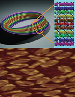
Figure 16 Typical nano architectures of a Möbius DNA strip: colored Möbius strip (top left) strip section (top right) and DNA image (bottom).29
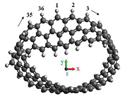
Figure 17 Graphene Möbius structure with length L = 18 and width N = 3. Möbius axis and edge C atom index are shown.31
From Equation 2, the properties of the Möbius transformation f(z) are

Figure 18 Spin-dependent density of states of graphene Möbius strip as a function of electron energy (a) and molecular orbital at E=0 eV (b).31
(i) f(z) can be expressed as a composition of affine transformations (scaling: z→tz, translation: z→z+p, rotation: z→eiθ z , complex conjugation: ![]() , inversion:
, inversion:  ), where t, p ∈ℂ
(ii) f(z) maps ℂ one-to-one onto itself, and is continuous
(iii) f(z) maps circles and lines to circles and lines
(iv) f(z) is conformal
From (i)-(iv), the family of functions is the composition of functions; the identity element is the identity map, and the inverse is given by inverse function. The Möbius group consists of those fractional linear transformations that map the open unit disk D={z∈ℂ:|z|<1} to itself in a one-to-one way. These transformations and their inverses are analytic on D and map its boundary, the unit circle S1={z∈ℂ:|z|<1} to itself. The automorphism of the disk is in the form:


where φ∈R , ψ∈R , and α∈D.
From Equations 1 through 5, the Möbius transformation can be used to achieve Möbius metamaterial symmetry, which has received widespread interest in the field of metamolecules, optical polarization, DNA sensing and high frequency components for energy saving electronics and instrumentation.26-35
EXAMPLES: MÖBIUS METAMATERIAL SYMMETRY
Benzene Metamolecules
The EM symmetry discovered in metamaterial is equivalent to the structural symmetry of a Möbius strip, with the number of twists controlled by the sign change of the electromagnetic coupling between the meta-atoms. Figure 14 illustrates metamaterial Möbius symmetry in metals and dielectrics.27 As shown in Figure 14, the hyperspace Möbius mechanism transforms ordinary benzene molecules into metamolecules with Möbius symmetry; “the topological phenomenon that yields a half-twisted strip with two surfaces but only one side.” The prototype of the metamolecular trimmer shown in Figure 14 is a 3-body system like a trimmer; metallic resonant meta-atoms configured as coupled split ring resonators (symbolized as metamolecules) exhibiting topological Möbius cyclic symmetry (C3-symmetry) through three rotations of 120 degrees. Möbius twists result from a change in the signs of the electromagnetic coupling constants between the constituent meta-atoms.27 The interesting phenomena is that “different coupling signs exhibit resonance frequencies that depend only on the number of turns but not the locations of the twists,’’ thus confirming its Möbius symmetry.

Figure 19 Möbius molecular rings made of carbon atoms (a) energy spectra Ekσ of the molecular ring (b) relative permittivity as a function of ∆ω (c) and relative permeability as a function of ∆ω (d).32
Polarized Light
Figure 15 illustrates the artificial Möbius strip formed by EM waves, which demonstrates that “a light-beam can be controlled so that its polarization twists follow a contour of Möbius strips.”28 The creation of EM waves around a Möbius contour is interesting for improving the fundamental understanding of optical polarization and the complex light beam engineering needed for developing optical micro- and nano-fabrication structures for sub-wavelength imaging. As shown in Figure 15, the typical Möbius strip surface consists of polarized states of a light beam, with a non-vanishing curvature, and exhibiting spatial symmetry.
DNA Strip Sensor
Figure 16 shows the nano-architectures of a Möbius DNA strip in which each colored band represents a different DNA double helix. Such nano-architectures can be used in high sensitivity biological and chemical sensing devices. 29
MMI Graphene
Graphene has received extensive attention recently due to its remarkable structural and superior electronic and optical properties.30 A single layer of graphite exhibits mechanical properties like thin paper or plastic with large bulk modulus along the graphene plane and is easily bent or curved. This unique characteristic allows graphene to wrap into carbon nanotubes without deformation and qualifies its use as a material for the construction of Möbius strips for microwave and optical components. The bandgap and cohesive energy of Möbius graphene as depicted in Figure 17 depends on the width of the strip, and is augmented by increasing the width, as described by 31
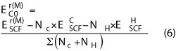
where the superscript r(M) corresponds to the graphene ribbon (Möbius strip), NC is the number of carbon atoms, NH is the number of hydrogen atoms,  is the self-consistent field energy of the graphene ribbon, and
  and
and  are the self-consistent field energy of the carbon and hydrogen atoms, respectively.
The magnetic moment and spin-properties of Möbius graphene are interesting. A graphene Möbius strip maintains its metallic surface states in the presence of an external electric field. For sufficiently higher applied electric field, spin flipping can take place in the Möbius strip. In contrast with graphene nanoribbons, graphene Möbius strips show half-semiconducting properties when an external electric field is applied. Figure 18 shows the typical orbital of a graphene Möbius strip and spin dependent density of states (DOS). The ferromagnetism and spin-flipping properties of Möbius graphene are attractive for spintronic devices and quantum oscillator applications.31
Figure 19 shows the characteristics of Möbius molecular rings that support metamaterial applications (negative permittivity ε and negative permeability).32 Two energy bands are denoted by their different pseudo spin labels σ = and ↓. Detuning ∆ω =ω-∆0.32 The difference between the Möbius molecular ring and the common annulenes lies in the boundary condition. The negative index properties offer remarkable properties such as image cloaking, sub-wavelength imaging and enhancement of evanescent fields resulting in improved Q-factor.
Figure 20 depicts the application of graphene Möbius strips for the realization of microelectronic components.30-35 It illustrates the next generation microwave components realized by Möbius metamaterial strips through the electromagnetic coupling dynamics governed by the Möbius transformation.
As shown in Figure 20, cylindrical closed ring structures formed by graphene nanoribbons possessing two edges exhibit anti-ferromagnetic (zero-magnetic moment), whereas Möbius closed-ring strips formed by graphene nanoribbons possessing a single-edge exhibit ferromagnetism (nonzero magnetic moment). Graphene nanoribbons with a ‘zigzag’ edge structure exhibit magnetism at their edges. The most stable configuration of these ribbons is anti-ferromagnetic, so that magnetic moments at opposite edges point in opposite directions, reducing the total magnetic moment of the ribbons to zero. However, a graphene Möbius strip has only one continuous edge, hence no magnetic cancellation between the opposite edges, resulting in a nonzero magnetic moment.
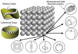
Figure 20 Structures of Möbius metamaterial strips formed by graphene for the realization of microelectronic components.30
Medical Telemetry
Medical telemetry systems have considerably increased due to the inevitability for early diagnoses of diseases and continuous monitoring of physiological parameters. Microwave antennas and sensors are key components of these telemetry systems since they provide the communication between the patient and base station. The Industrial, Scientific and Medical (ISM) radio bands are portions of the radio spectrum reserved internationally for the use of RF energy for industrial, scientific and medical purposes other than communications. Through the use of metamaterial like EBG structures in slotted microstrip antennas, increased efficiency and better return loss characteristics can be achieved.36
Cancer is the uncontrolled growth of abnormal (malignant) cells. Integrating microwave designs with metamaterial-inspired structures can lead to cost-effective devices that can localize abnormalities within the human body with high precision. The basic principle behind cancer detection is that small changes in the water content of biological tissues produces changes in their permittivities (ε) and conductivities (σ).37 Malignant cells have significantly higher water content than normal tissues. Hence the permittivity and conductivity of a tumor are higher than those ones of normal tissues at microwave frequencies. A proposed biosensor consists of an array of complementary metallic metamaterial resonators. The reason for choosing split ring resonators (SRR) is their strong response to an electromagnetic field.37 An electromagnetic source generates an electromagnetic wave impinging on a metamaterial array and a detector is placed so as to detect the signal after the array. The biosensor without any material under test has a specific resonant frequency.37 The variation in permittivity of the material under test, acts on the capacitance of the resonators, shifting with high sensitivity the sensor resonant frequency. Thus the shift in resonant frequency and the shape of the response is extremely useful for tumor detection. Figure 21a shows a typical metamaterial-inspired coupled SRR based sensor comprising 12 SRRs. Figure 21b represents a pixel within the sensor.
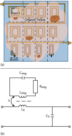
Figure 21 Metamaterial inspired microstrip coupled SSR sensor array (a) and equivalent circuit of a SRR loaded microstrip element (b).27-28
If, for example, an organic tissue, interacts with the outer split of a SRR it changes its capacitance value due to a change of effective permittivity. In this way, differences in tissues, such as abnormalities, can be detected.38 The equivalent circuit of a microstrip line loaded with a single SRR for the quasi-static case is shown in Figure 21b.39 The SRR is magnetically coupled to the transmission line with the coupling factor S, where Lo and Co correspond to the total SRR inductance and capacitance, respectively. The equivalent circuit yields the effective permeability with Lorentz dispersion40

with p being the net cell length.
Acoustic Imaging
Acoustic imaging tools are used in both medical diagnostics and in testing the structural integrity of everything from airplanes to bridges. Medical personnel and structural engineers often need to focus sound for imaging or therapeutic purposes. Metamaterial gives researchers more control over the angle at which acoustic waves can pass through it. Figure 22 shows a typical metamaterial inspired acoustic hyperbolic structure made of paper and aluminum for acoustic imaging application. The acoustic hyperbolic metamaterial (AHM) structure allows manipulation of acoustic waves to more than double the resolution of acoustic imaging by focusing acoustic waves and controlling the angles at which sound passes through the metamaterial.41 It interacts with acoustic waves in two different ways. From one direction, it exhibits a positive density and interacts with acoustic waves normally, just like air. But from a perpendicular direction, the metamaterial exhibits a negative density. This effectively makes acoustic waves bend at angles that are the exact opposite of what basic physics predicts. This has some very useful applications. For one, it can be used to improve acoustic imaging. Traditionally, acoustic imaging cannot achieve image resolution smaller than half of a sound’s wavelength. For example, an acoustic wave of 100 kHz, traveling through air has a wavelength of 3.4 mm, limiting image resolution to 1.7 mm.
CONCLUSION
The unique features of MMI structures open the gateway to new inventions, recurring in an endless fashion; one could say that the future has the form of an MMI surface. In this article, the Casimir effect is discussed briefly. Details of the Casimir effect and applications using MMI structures for futuristic applications will be discussed in parts 2 and 3.
References
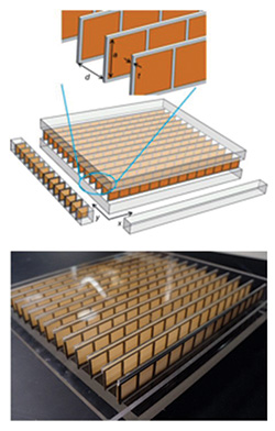
Figure 22 Physical structure of acoustic hyperbolic metamaterial.
- U. L. Rohde and A. K. Poddar, “Möbius Strips and Metamaterial Symmetry: Theory and Applications,” Microwave Journal, Vol. 11, No. 57, November 2014, pp. 76–88.
- U. L. Rohde and A. K. Poddar, “Metamaterial Resonators: Theory and Applications,” Microwave Journal, Vol. 57, No. 2, December 2014, p. 74.
- U. L. Rohde and A. K. Poddar, “Metamaterial Möbius Strip Resonators for Tunable Oscillators, Part 3,” Microwave Journal, Vol. 58, No. 1, January 2015, p. 64.
- A. Poddar, “Slow Wave Resonator Based Tunable Multi-Band Multi-Mode Injection-Locked Oscillator,” Habil Thesis, BTU Cottbus, Germany, 2014.
- U. L. Rohde, A. K. Poddar and D. Sundarrajan, “Real Time Signal Retention Device Using Co-Planar Waveguide (CPW) as Möbius Strip,” IEEE MTT-S Digest, June 2013, pp. 1–3.
- U. L. Rohde, A. K. Poddar and D. Sundarrajan, “A Novel Möbius-Coupled Printed Resonator Based Signal Sources,” IEEE MTT-S Digest, June 2013, pp. 1–3.
- C. Caloz, “Perspectives on EM Metamaterials,” Materials Today, Vol. 12, No. 3, March 2009, pp. 12–20.
- C. Caloz, “Tomorrow’s Metamaterials: Manipulation of Electromagnetic Waves in Space, Time and Space-time,” February 2016, http://arxiv.org/pdf/1602.04340.pdf.
- A. Lambrecht, “The Casimir Effect: A Force From Nothing,” Physics World, September 2002, https://www.physics.ohio-state.edu/~jay/631/Casimir%20effect.pdf.
- R. Zeng, Y. Chen and Y. Yang, “Stable Multilayer Structure Based on Restoring Casimir Forces,” European Physical Journal B, Vol. 86, No. 398, September 2013, pp. 1–6.
- F. Intravaia and C. Henkel, “Can Surface Plasmons Tune the Casimir Forces Between Metamaterials?,” New Frontiers in Casimir Force Control, Poster, September 2009, http://cnls.lanl.gov/casimir/PostersSF/Intravaia-SantaFe-poster.pdf.
- U. Leonhardt and T. G. Philbin, “Quantum Levitation by Left-Handed Metamaterials,” New Journal of Physics, Vol. 9, August 2007.
- J. Q. Quach, “Gravitational Casimir Effect,” Physical Review Letters, Vol. 114, February 2015.
- “Internet of Things,” Wikipedia, https://en.wikipedia.org/wiki/Internet_of_Things.
- C. Caloz, “Metamaterial Dispersion Engineering Concepts and Applications,”Proceedings of the IEEE, Vol. 99, No. 10, October 2011, pp. 1711–1719.
- B. E. A. Saleh and M. C. Teich, Fundamentals of Photonics, 2nd ed., Wiley, 1964, Chap. 22.
- C. Caloz, S. Gupta, Q. Zhang and B. Nikfal, “Analog Signal Processing,” IEEE Microwave Magazine, Vol. 14, No. 6, September 2013, pp. 87–103.
- “ESTCube-1,” Wikipedia, https://en.wikipedia.org/wiki/ESTCube-1.
- “Hermes CubeSat Mission,” Earth Observation Portal, https://directory.eoportal.org/web/eoportal/satellite-missions/h/hermes.
- “CubeSats,” NASA, www.nasa.gov/mission_pages/cubesats/index.html.
- “NASA CubeSat launch,” Southgate Amateur Radio News, http://southgatearc.org/news/january2010/nasa_cubesat_launch.htm.
- G. L. Skrobot, “Project ElaNa and NASA’s CubeSat Initiative,” Proceedings of the Cal Poly 2010 CubeSat Developer’s Workshop, April 2010.
- O. Ceylan, A. Caglar, H. B. Tugrel, H. O. Cakar, A. O. Kislal, K. Kula and H. B. Yagci, “Small Satellites Rock,” IEEE Microwave Magazine, Vol. 17, No. 3, March 2016, pp. 26–33.
- “Metamaterials Approach Makes Better Satellite Antennas,” phys.org, January 2011, http://phys.org/news/2011-01-metamaterials-approach-satellite-antennas.html.
- E. Hückel, “Grundzüge der Theorie Ungesättiger und Aromatischer Verbindungen,” Zeitschrift für Elektrochemie und Angewandte Physikalische Chemie, Vol. 43, No. 9, September 1937, pp. 77–85.
- S. A. Marvel, R. E. Mirollo and S. H. Strogatz, “Identical Phase Oscillators with Global Sinusoidal Coupling Evolve by Möbius Group Action,” American Institute of Physics,Vol. 19, No. 4, October 2009, pp. 043104-1-11.
- C.W. Chang, M. Liu, S. Nam, S. Zhang, Y. Liu, G. Bartal, and X. Zhang, “Optical Möbius Symmetry in Metamaterials,” Physical Review Letters, Vol. 105, December 2010, pp. 23550-1–4.
- T. Bauer1, P. Banzer, E. Karimi, S. Orlov, A. Rubano, L. Marrucci, E. Santamato, R. W. Boyd and G. Leuchs, “Observation of Optical Polarization Möbius Strips,” Science, Vol. 347, No. 6225, February 2015, pp. 964–966.
- D. Han, S. Pal, Y. Liu and H. Yan, “Folding and Cutting DNA into Reconfigurable Topological Nanostructures,” Nature Nanotechnology, Vol. 5, October 2010, pp. 712–717.
- X. Wang, X. Zheng, M. Ni, L. Zou and Z. Zeng, “Theoretical Investigation of Möbius Strips Formed from Graphene,” Applied Physics Letters, Vol. 97, September 2010.
- H. Mazidabadi, H. Simchi and M. Esmaeilzadeh, “Electronic and Magnetic Properties of Graphene Möbius Strips: Density Functional Theory Approach,” Journal of Nanoscience and Nanotechnology, Vol. 3, No. 5, September 2014, pp. 268–273.
- Y. N. Fang, Y. Shen, Q. Ai and C. P. Sun, “Negative Refraction Induced by Möbius Topology,” Cornell University Library, January 2015.
- A. Poddar, “Slow Wave Resonator Based Tunable Multi-Band Multi-Mode Injection-Locked Oscillator,” Habil Thesis, BTU Cottbus, Germany, 2014.
- G. Li and E. Afshari, “A Low Phase Noise Multi-Phase Oscillator Based on Left-Handed LC-Ring,” IEEE Journal of Solid State Circuits, JSSC. Vol. 45, No. 9, September 2010, pp. 1822–1833.
- A. Rofougaran, J. Rael, M. Rofougaran and A. Abidi, “A 900 MHz CMOS LC Oscillator with Quadrature Outputs,” IEEE International Solid State Circuits Conference, February 1996, pp. 392–393.
- H. Kumar, R. K. Kanth, P. Liljeberg and H. Tenhunen, “Metamaterial Based Slotted Patch Antenna,” IEEE 10thInternational Conference on Telecommunication in Modern Satellite Cable and Broadcasting Services, Vol. 1, October 2011, pp. 43–46.
- L. La Spada, F. Bilotti and L. Vegni, “Metamaterial Biosensor for Cancer Detection,” IEEE Sensors, October 2011, pp. 627–630.
- M. Puentes, M. Maasch, M. Schubler and R. Jakoby, “Frequency Multiplexed 2-Dimensional Sensor Array Based on Split-Ring Resonators for Organic Tissue Analysis,” IEEE Transactions on Microwave Theory and Techniques, Vol. 60, No. 6, June 2012, pp. 1720–1727.
- J. Baena, J. Bonache, F. Martin, R. Sillero, F. Falcone, T. Lopetegi, M. Laso, J. Garcia-Garcia, I. Gil, M. Portillo and M. Sorolla, “Equivalent Circuit Models for Split-Ring Resonators and Complementary Split-Ring Resonators Coupled to Planar Transmission Lines,” IEEE Transactions on Microwave Theory and Techniques, Vol. 53, No. 4, April 2005, pp. 1451–1461.
- A. Trehan and N. Nikolova, “Summary of Materials and Recipes Available in the Literature to Fabricate Biological Phantoms for RF and Microwave Experiments,” Ph.D. dissertation, McMaster University, ON, Canada, 2009.
- C. Shen, Y. Xie, N. Sui, W. Wang, S. A. Cummer and Y. Jing, “Broadband Acoustic Hyperbolic Metamaterial,” Physical Review Letters, Vol. 115, December 2015.